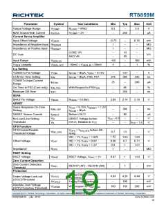
RT8859M
Parameter
Symbol
VDVDx
VDVDHYS
tUVLO
Test Conditions
VDVDx Threshold
Min
1.01
--
Typ
1.06
25
Max
1.11
--
Unit
V
Divided Input Voltage
Detection (DVDx)
Threshold
Falling Edge Hysteresis
Rising Above Threshold
mV
μs
Delay of UVLO, DVDx
--
3
--
VISENxN Rising Above Threshold, Pin
OFS Disable
Delay of OVP
tOV
--
1
--
μs
Measured at ISEN1N/ISENAN with
respect to unloaded output voltage
(UOV) (for 0.8 < UOV < 1.52)
Under Voltage Protection
(UVP) Threshold
VUV
−350 −300 −250
mV
Delay of UVP
tUVP
VNVP
tNVP
VISENxN Falling below Threshold
After OVP, Falling Edge
--
−100
--
3
−50
1
--
--
--
μs
mV
μs
Negative Voltage
Protection Threshold
Delay of NVP
VISENxN Falling below Threshold
GILIMIT = VOCSET / (VISENxP
− VISENxN), VOCSET = 2.400V,
(VISENxP − VISENxN) = 50mV
43.2
48
52.8
Current Limit Gain Setting
(per phase)
GILIMIT
V/V
GILIMITA = VOCSETA / (VISENAP
− VISENAN), VOCSETA = 2.4V, (VISENAP 43.2
− VISENAN) = 50mV
48
15
52.8
--
Current Limit Latch
Counter (per phase)
NILIM
Times of UGATE Rising
--
Times
V
EN Input
Logic-High VIH
Logic-Low VIL
0.7
--
--
--
--
Threshold
Voltage
0.3
Logic Inputs
EN Hysteresis
VENHYS
IEN
--
30
--
--
1
mV
Leakage Current of EN
VCLK, VDIO
Input
Threshold
Voltage
−1
μA
Logic-High VIH
0.665
--
--
V
Logic-Low VIL
--
--
--
70
--
0.367
VCLK,VDIO Hysteresis
VHYS
--
1
mV
Leakage Current of
ADD,VCLK,VDIO
ILEAK_IN
−1
μA
ALERT
I
ALERT = 10mA
ALERT Low Voltage
Power On Sequence
VALERT
--
--
--
--
0.13
2
V
From EN = high until VR Controller is
ready to accept SVID command
SVID Ready Delay Time
tA
ms
VR_RDY Trip Threshold
VR_RDY Low Voltage
VR_RDY Delay
VTH_VR_RDY VISENxN − 1st VDAC
--
--
--
−100
--
--
0.4
--
mV
V
VVR_RDY
tVR_RDY
IVR_RDY = 4mA
VISENxN = VINITIAL to VR_RDY High
100
μs
Copyright 2012 Richtek Technology Corporation. All rights reserved.
©
is a registered trademark of Richtek Technology Corporation.
www.richtek.com
20
DS8859M-05 July 2012

 RICHTEK [ RICHTEK TECHNOLOGY CORPORATION ]