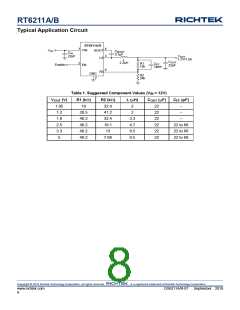
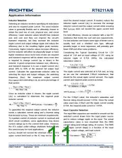
RT6211A/B
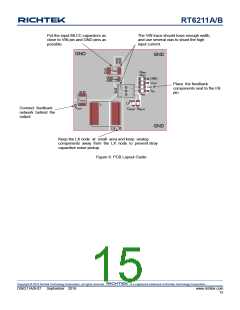
Put the input MLCC capacitors as
close to VIN pin and GND pins as
possible.
The VIN trace should have enough width,
and use several vias to shunt the high
input current.
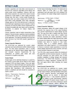
GND
GND
CIN1
CIN2
RFB2
RFB1
GND
VOUT
CFF
Place the feedback
components next to the FB
pin.
1
VIN
REN
COUT1
VOUT
LX
CBOOT RBOOT
L
Connect feedback
network behind the
output
GND
LX
Keep the LX node at small area and keep analog
components away from the LX node to prevent stray
capacitive noise pickup.
Figure 8. PCB Layout Guide
Copyright © 2018 Richtek Technology Corporation. All rights reserved.
is a registered trademark of Richtek Technology Corporation.
DS6211A/B-07 September 2018
www.richtek.com
15

 RICHTEK [ RICHTEK TECHNOLOGY CORPORATION ]