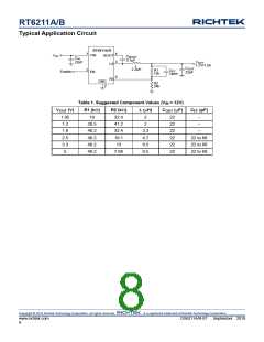
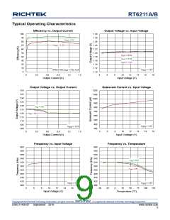
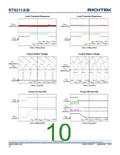
RT6211A/B
For output voltage accuracy, use divider resistors with
Thermal Considerations
1% or better tolerance.
For continuous operation, do not exceed absolute
maximum junction temperature. The maximum power
dissipation depends on the thermal resistance of the IC
package, PCB layout, rate of surrounding airflow, and
difference between junction and ambient temperature.
The maximum power dissipation can be calculated by
the following formula :
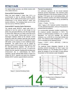
External BOOT Bootstrap Diode
When the input voltage is lower than 5.5V it is
recommended to add an external bootstrap diode
between VIN (or VINR) and the BOOT pin to improve
enhancement of the internal MOSFET switch and
improve efficiency. The bootstrap diode can be a low
cost one such as 1N4148 or BAT54.
PD(MAX) = (TJ(MAX) TA) / JA
where TJ(MAX) is the maximum junction temperature,
TA is the ambient temperature, and JA is the junction to
ambient thermal resistance.
External BOOT Capacitor Series Resistance
The internal power MOSFET switch gate driver is
optimized to turn the switch on fast enough for low
power loss and good efficiency, but also slow enough
to reduce EMI. Switch turn-on is when most EMI occurs
since VLX rises rapidly. During switch turn-off, LX is
discharged relatively slowly by the inductor current
during the dead time between high-side and low-side
switch on-times. In some cases it is desirable to reduce
EMI further, at the expense of some additional power
dissipation. The switch turn-on can be slowed by
placing a small (<47) resistance between BOOT and
the external bootstrap capacitor. This will slow the
high-side switch turn-on and VLX's rise. To remove the
resistor from the capacitor charging path (avoiding poor
enhancement due to undercharging the BOOT
capacitor), use the external diode shown in Figure 6 to
charge the BOOT capacitor and place the resistance
between BOOT and the capacitor/diode connection.
For recommended operating condition specifications,
the maximum junction temperature is 125C. The
junction to ambient thermal resistance, JA, is layout
dependent. For SOT-23-6 package, the thermal
resistance, JA, is 80C/W on a four-layer Richtek test
board. The maximum power dissipation at TA = 25C
can be calculated by the following formula :
PD(MAX) = (125C 25C) / (80C/W) = 1.25W for
SOT-23-6 package
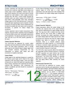
The maximum power dissipation depends on the
operating ambient temperature for fixed TJ(MAX) and
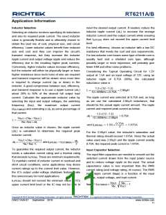
thermal resistance, JA. The derating curve in Figure 7
allows the designer to see the effect of rising ambient
temperature on the maximum power dissipation.
2.0
Four-Layer PCB
1.8
1.6
1.4
1.2
1.0
0.8
0.6
0.4
0.2
0.0
5V
BOOT
RT6211A/B
LX
0.1μF
Figure 6. External Bootstrap Diode
0
25
50
75
100
125
Ambient Temperature (°C)
Figure 7. Derating Curve of Maximum Power
Dissipation
Copyright © 2018 Richtek Technology Corporation. All rights reserved.
is a registered trademark of Richtek Technology Corporation.
www.richtek.com
14
DS6211A/B-07 September 2018

 RICHTEK [ RICHTEK TECHNOLOGY CORPORATION ]