RT6211A/B
steady-state stability of the circuit. Choose a suitable
capacitor value that following below step.
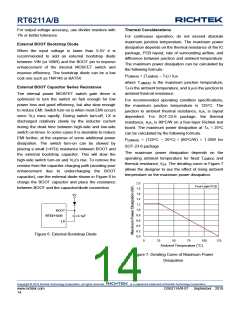
connected to EN to create an additional input under
voltage lockout threshold (Figure 4).
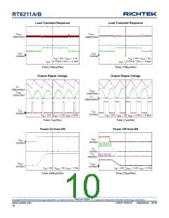
Get the BW the quickest method to do transient
response form no load to full load. Confirm the
damping frequency. The damping frequency is BW.
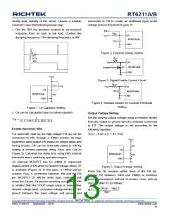
EN
R
EN
V
EN
RT6211A/B
IN
C
EN
GND
Figure 2. External Timing Control
R
EN
100k
BW
V
EN
RT6211A/B
GND
IN
Q1
Enable
V
OUT
Figure 3. Digital Enable Control Circuit
R
EN1
R1
C
V
ff
IN
EN
FB
RT6211A/B
R
EN2
RT6211A/B
GND
R2
GND
Figure 4. Resistor Divider for Lockout Threshold
Setting
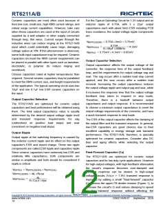
Figure 1. Cff Capacitor Setting
Cff can be calculated base on below equation :
Output Voltage Setting
Set the desired output voltage using a resistive divider
from the output to ground with the midpoint connected
to FB. The output voltage is set according to the
following equation :
1
C
ff
23.1412R1BW0.8
Enable Operation (EN)
For automatic start-up the high-voltage EN pin can be
connected to VIN, through a 100k resistor. Its large
hysteresis band makes EN useful for simple delay and
timing circuits. EN can be externally pulled to VIN by
adding a resistor-capacitor delay (REN and CEN in
Figure 2). Calculate the delay time using EN's internal
threshold where switching operation begins.
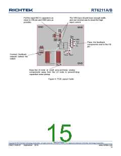
VOUT = 0.8V x (1 + R1 / R2)
V
OUT
R1
FB
RT6211A/B
R2
GND
An external MOSFET can be added to implement
digital control of EN when no system voltage above 2V
is available (Figure 3). In this case, a 100k pull-up
resistor, REN, is connected between VIN and the EN
pin. MOSFET Q1 will be under logic control to pull
down the EN pin. To prevent enabling circuit when VIN
is smaller than the VOUT target value or some other
desired voltage level, a resistive voltage divider can be
placed between the input voltage and ground and
Figure 5. Output Voltage Setting
Place the FB resistors within 5mm of the FB pin.
Choose R2 between 10k and 100k to minimize
power consumption without excessive noise pick-up
and calculate R1 as follows :
R2(VOUT VREF
)
R1
VREF
Copyright © 2018 Richtek Technology Corporation. All rights reserved.
is a registered trademark of Richtek Technology Corporation.
DS6211A/B-07 September 2018
www.richtek.com
13

 RICHTEK [ RICHTEK TECHNOLOGY CORPORATION ]