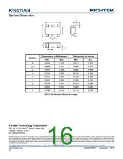
RT6211A/B
Ceramic capacitors are most often used because of
their low cost, small size, high RMS current ratings, and
robust surge current capabilities. However, take care
when these capacitors are used at the input of circuits
supplied by a wall adapter or other supply connected
through long, thin wires. Current surges through the
inductive wires can induce ringing at the RT6211A/B
input which could potentially cause large, damaging
voltage spikes at VIN. If this phenomenon is observed,
some bulk input capacitance may be required. Ceramic
capacitors (to meet the RMS current requirement) can
be placed in parallel with other types such as tantalum,
electrolytic, or polymer (to reduce ringing and
overshoot).
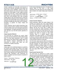
For the Typical Operating Circuit for 1.2V output and an
inductor ripple of 0.75A, with 2 x 22F output
capacitance each with about 5m ESR including PCB
trace resistance, the output voltage ripple components
are :
V
= 0.75A5m = 3.75mV
RIPPLE(ESR)
0.75A
844μF500kHz
V
=
= 4.3mV
RIPPLE(C)
V
= 3.75mV 4.3mV = 8.05mV
RIPPLE
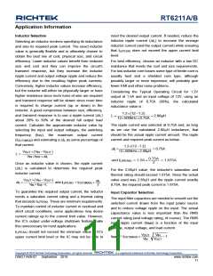
Output Capacitor Selection
Output capacitance affects the output voltage of the
converter, the response time of the output feedback
loop, and the requirements for output voltage sag and
soar. The sag occurs after a sudden load step current
applied, and the soar occurs after a sudden load
removal. Increasing the output capacitance reduces
the output voltage ripple and output sag and soar, while
Choose capacitors rated at higher temperatures than
required. Several ceramic capacitors may be paralleled
to meet the RMS current, size, and height requirements
of the application. The typical operating circuit uses two
10F and one 0.1F low ESR ceramic capacitors on
the input.
it increases the response time that the output voltage
feedback loop takes to respond to step loads,
Output Capacitor Selection
Therefore, there is
a
tradeoff between output
capacitance and output response. It is recommended
to choose a minimum output capacitance to meet the
output voltage requirements of the converter, and have
a quick transient response to step loads.
The RT6211A/B are optimized for ceramic output
capacitors and best performance will be obtained using
them. The total output capacitance value is usually
determined by the desired output voltage ripple level
and transient response requirements for sag
(undershoot on positive load steps) and soar
(overshoot on negative load steps).
The ESR of the output capacitor affects the damping of
the output filter and the transient response. In general,
low-ESR capacitors are good choices due to their
excellent capability in energy storage and transient
performance. The RT6211A/B, therefore, is specially
optimized for ceramic capacitors. Consider also DC
bias and aging effects while selecting the output
capacitor.
Output Ripple
Output ripple at the switching frequency is caused by
the inductor current ripple and its effect on the output
capacitor's ESR and stored charge. These two ripple
components are called ESR ripple and capacitive ripple.
Since ceramic capacitors have extremely low ESR and
relatively little capacitance, both components are
similar in amplitude and both should be considered if
ripple is critical.
Feed-Forward Capacitor (Cff)
The RT6211A/B are optimized for ceramic output
capacitors and for low duty cycle applications. However
for high-output voltages, with high feedback attenuation,
the circuit's response becomes over-damped and
transient response can be slowed. In high-output
voltage circuits (VOUT > 1.8V) transient response is
improved by adding a small “feed-forward” capacitor
(Cff) across the upper FB divider resistor (Figure 1), to
increase the circuit's Q and reduce damping to speed
up the transient response without affecting the
V
= V
V
RIPPLE
RIPPLE(ESR) RIPPLE(C)
V
= I R
RIPPLE(ESR)
L
ESR
I
L
V
=
RIPPLE(C)
8C
f
OUT SW
Copyright © 2018 Richtek Technology Corporation. All rights reserved.
is a registered trademark of Richtek Technology Corporation.
www.richtek.com
12
DS6211A/B-07 September 2018

 RICHTEK [ RICHTEK TECHNOLOGY CORPORATION ]