RX62Nグループ、RX621グループ
5. Electrical Characteristics
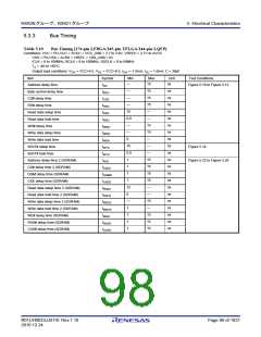
Table 5.11
Bus Timing [100-pin LQFP/85-pin TFLGA]
Conditions: VCC = PLLVCC = AVCC = VCC_USB = 2.7 to 3.6V, VREFH = 2.7V to AVCC
VSS = PLLVSS = AVSS = VREFL = VSS_USB = 0V
ICLK = 8 to 100MHz, PCLK = 8 to 50MHz, BCLK = 8 to 50MHz
Ta = -40 to +85C
Output load conditions: VOH = VCC × 0.5, VOL = VCC × 0.5, IOH = -1.0mA, IOL = 1.0mA, C = 30pF
Item
Symbol
tAD
Min.
—
Max.
30
Unit
ns
Test Conditions
Address delay time
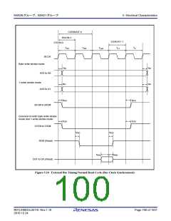
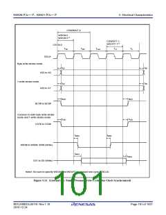
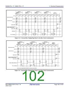
Figure 5.10 to Figure 5.13
Byte control delay time
CS# delay time
tBCD
tCSD
tRSD
tRDS
tRDH
tWRD
tWDD
tWDH
tWTS
tWTH
—
—
—
15
0.0
—
—
0
30
30
30
—
—
30
35
—
—
—
ns
ns
ns
ns
ns
ns
ns
ns
ns
ns
RD# delay time
Read data setup time
Read data hold time
WR# delay time
Write data delay time
Write data hold time
WAIT# setup time
WAIT# hold time
15
0.0
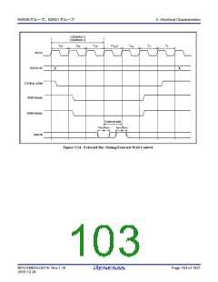
Figure 5.14
R01UH0033JJ0110 Rev.1.10
2010.12.24
Page 99 of 1931

 RENESAS [ RENESAS TECHNOLOGY CORP ]