RX62Nグループ、RX621グループ
5. Electrical Characteristics
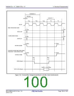
CSRWAIT:2
RDON:1
CSPRWAIT:2
RDON:1
CSPRWAIT:2
RDON:1
CSPRWAIT:2
RDON:1
CSROFF:1
CSON:0
TW1
TW2
Tend
Tpw1
Tpw2
Tend
Tpw1
Tpw2
Tend
Tpw1
Tpw2
Tend
Tn1
Th
BCLK
Byte write strobe mode
tAD
tAD
tAD
tAD
tAD
A23 to A0
1-write strobe mode
tAD
tAD
tAD
tAD
tAD
A23 to A1
tBCD
tBCD
BC3# to BC0#
Common to both byte write strobe
mode and 1-write strobe mode
tCSD
tCSD
CS7# to CS0#
tRSD
tRSD
tRSD
tRSD
tRSD
tRSD
tRSD
tRSD
RD# (Read)
tRDS
tRDH
tRDS
tRDH
tRDS
tRDH
tRDS
tRDH
D31 to D0 (Read)
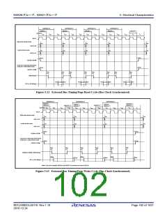
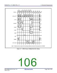
Figure 5.12 External Bus Timing/Page Read Cycle (Bus Clock Synchronized)
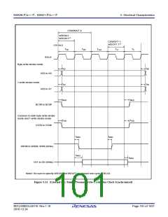
CSPWWAIT:2
CSWWAIT:2
WRON:1
WDON:1*1
CSON:0
CSPWWAIT:2
CSWOFF:1
WRON:1
WRON:1
WDOFF:1*1
Tdw1
WDOFF:1*1
Tn1
WDOFF:1*1
Tdw1
WDON:1*1
Tpw1
WDON:1*1
Tpw1
TW2
Tend
Tpw2
Tpw2
TW1
Tend
Tend
Th
BCLK
Byte write strobe mode
tAD
tAD
tAD
tAD
A23 to A0
1-write strobe mode
tAD
tAD
tAD
tAD
A23 to A1
tBCD
tBCD
BC3# to BC0#
Common to both byte write strobe
mode and 1-write strobe mode
tCSD
tCSD
CS7# to CS0#
tWRD
tWRD
tWRD
tWRD
tWRD
tWRD
WR3# to WR0#, WR# (Write)
D31 to D0 (Write)
tWDD
tWDD
tWDD
tWDH
tWDH
tWDH
Note1: Be sure to specify WDON and WDOFF as at least one cycle of BCLK.
Figure 5.13 External Bus Timing/Page Write Cycle (Bus Clock Synchronized)
R01UH0033JJ0110 Rev.1.10
2010.12.24
Page 102 of 1931

 RENESAS [ RENESAS TECHNOLOGY CORP ]