RX62Nグループ、RX621グループ
5. Electrical Characteristics
5.3.2
Control Signal Timing
Table 5.9
Control Signal Timing
Conditions: VCC = PLLVCC = AVCC = VCC_USB = 2.7 to 3.6V, VREFH = 2.7V to AVCC
VSS = PLLVSS = AVSS = VREFL = VSS_USB = 0V
Ta = -40 to +85C
Item
Symbol
Min.
20
Max.
—
Unit
tIcyc
Test Conditions
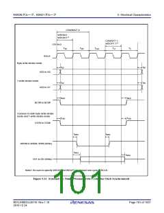
Figure 5.7
*2
RES# pulse width
tRESW
(except for programming or erasure of the ROM or data-flash memory
1.5
—
µs
or blank checking of the data-flash memory*1
)
Internal reset time*3
tRESW2
tNMIW
tIRQW
35
—
—
—
µs
ns
ns
NMI pulse width
200
200
Figure 5.8
Figure 5.9
IRQ pulse width
Note 1. Do not allow a reset by the signal on the RES# pin during programming or erasure of the ROM or data-flash memory or during
blank checking of the data-flash memory. For details, see section 37.13, Usage Notes, in section 37., ROM (Flash Memory for
Code Storage).
Note 2. Both the time and the number of cycles should satisfy the specifications.
Note 3. This is to specify the FCU reset and the WDT reset.
Note 4. tIcyc: ICLK cycles
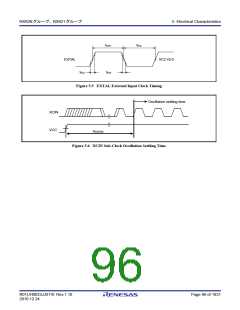
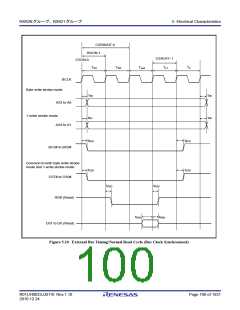
RES#
tRESW
Figure 5.7 Reset Input Timing
NMI
tNMIW
Figure 5.8 NMI Interrupt Input Timing
IRQ
tIRQW
Figure 5.9 IRQ Interrupt Input Timing
R01UH0033JJ0110 Rev.1.10
2010.12.24
Page 97 of 1931

 RENESAS [ RENESAS TECHNOLOGY CORP ]