RX62Nグループ、RX621グループ
5. Electrical Characteristics
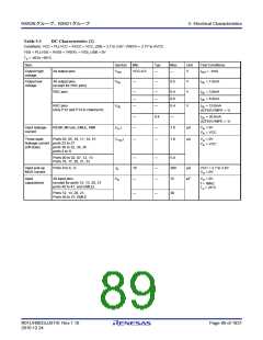
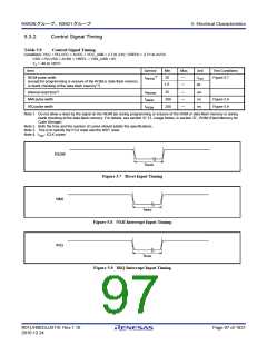
5.3.1
Clock Timing
Table 5.8
Clock Timing
Conditions: VCC = PLLVCC = AVCC = VCC_USB = 2.7 to 3.6V, VREFH = 2.7V to AVCC
VSS = PLLVSS = AVSS = VREFL = VSS_USB = 0V
Ta = -40 to +85C
Item
Symbol
tBcyc
Min.
20
Max.
125
Unit
ns
Test Conditions
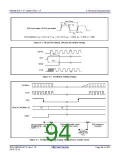
Figure 5.1
BCLK pin output cycle time
[176-pin LFBGA/145-pin TFLGA/144-pin LQFP]
BCLK pin output cycle time
[100-pin LQFP/85-pin TFLGA]
tBcyc
40
125
ns
BCLK pin output high pulse width
BCLK pin output low pulse width
BCLK pin output rising time
tCH
5
—
—
5
ns
ns
ns
ns
ns
ns
ns
ns
ns
ms
ms
tCL
5
tCr
—
—
20
5
BCLK pin output falling time
tCf
5
SDCLK pin output cycle time
tSDcyc
tCH
125
—
—
5
SDCLK pin output high pulse width
SDCLK pin output low pulse width
SDCLK pin output rising time
tCL
5
tCr
—
—
10
10
SDCLK pin output falling time
Oscillation settling time after reset (crystal)
tCf
5
tOSC1
tOSC2
—
—
Figure 5.2
Figure 5.3
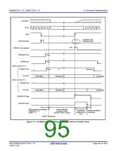
Oscillation settling time after leaving software standby mode
(crystal)
Oscillation settling time after leaving deep software standby mode
(crystal)
tOSC3
10
—
ms
Figure 5.4
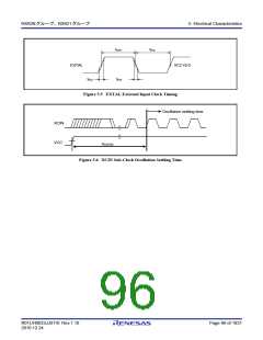
EXTAL external clock output delay settling time
EXTAL external clock input low pulse width
EXTAL external clock input high pulse width
EXTAL external clock rising time
tDEXT
tEXL
1
—
—
ms
ns
Figure 5.2
Figure 5.5
35.71
35.71
—
tEXH
—
ns
tEXr
5
ns
EXTAL external clock falling time
tEXf
—
5
ns
XCIN sub-clock oscillation settling time
XCIN sub-clock oscillation frequency
tSUBOSC
fSUB
2
—
s
Figure 5.6
32.768
62.5
—
kHz
kHz
On-chip oscillator (IWDTCLK) oscillation frequency
fIWDTCLK
187.5
R01UH0033JJ0110 Rev.1.10
2010.12.24
Page 93 of 1931

 RENESAS [ RENESAS TECHNOLOGY CORP ]