RX62Nグループ、RX621グループ
5. Electrical Characteristics
5.6
D/A Conversion Characteristics
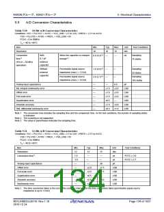
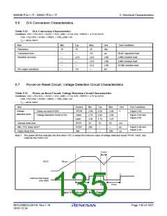
Table 5.22
D/A Conversion Characteristics
Conditions: VCC = PLLVCC = AVCC = VCC_USB = 2.7 to 3.6V, VREFH = 2.7V to AVCC
VSS = PLLVSS = AVSS = VREFL = VSS_USB = 0V
Ta = -40 to +85C
Item
Min.
10
—
Typ.
10
Max.
10
Unit
bits
µs
Test Conditions
Resolution
Conversion time
Absolute accuracy
—
3.0
20-pF capacitive load
2-MΩ resistive load
4-MΩ resistive load
10-MΩ resistive load
—
±2.0
—
±4.0
±3.0
±2.0
—
LSB
LSB
LSB
kΩ
—
—
—
RO output resistance
—
3.6
5.7
Power-on Reset Circuit, Voltage Detection Circuit Characteristics
Table 5.23
Power-on Reset Circuit, Voltage Detection Circuit Characteristics
Conditions: VCC = PLLVCC = AVCC = VCC_USB = 2.7 to 3.6V, VREFH = 2.7V to AVCC
VSS = PLLVSS = AVSS = VREFL = VSS_USB = 0V
Ta = -40 to +85C
Item
Symbol
VPOR
Vdet1
Vdet2
tPOR
tVOFF
tdet
Min.
2.48
2.75
3.05
20
Typ.
2.58
2.85
3.15
35
Max.
2.68
2.95
3.25
50
Unit
Test Conditions
Figure 5.63
Voltage
Power-on reset (POR)
V
detection level
Voltage detection circuit (LVD)
Figure 5.64 and
Figure 5.65
Internal reset time
ms
µs
µs
Min. VCC down time*1
Reply delay time
200
—
—
—
Figure 5.64 and
Figure 5.65
—
200
Note 1. The power-off time indicates the time when VCC is below the minimum value of voltage detection levels VPOR, Vdet1, and
Vdet2 for the POR/ LVD.
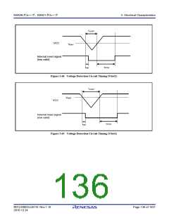
tVOFF
VCC
VPOR
Internal reset signal
(low valid)
tPOR
Figure 5.63 Power-on Reset Timing
tPOR
tdet
R01UH0033JJ0110 Rev.1.10
2010.12.24
Page 135 of 1931

 RENESAS [ RENESAS TECHNOLOGY CORP ]