RX62Nグループ、RX621グループ
5. Electrical Characteristics
5.4
USB Characteristics
Table 5.19
Internal USB Full-Speed Characteristics (DP, DM Pin Characteristics)
Conditions: VCC = PLLVCC = AVCC = VCC_USB = 3.0 to 3.6V, VREFH = 3.0V to AVCC
VSS = PLLVSS = AVSS = VREFL = VCC_USB = 0V
PCLK = 24 to 50MHz
Ta = -40 to +85C
Item
Symbol
VIH
Min.
2.0
Max.
—
Unit
V
Test Conditions
Input
Input high level voltage
Input low level voltage
Differential input Sensitivity
Differential commom mode range
Output high level voltage
Output low level voltage
Cross over voltage
Figure 5.61 and
Figure 5.62
characteristics
VIL
—
0.8
—
V
VDI
VCM
VOH
VOL
VCRS
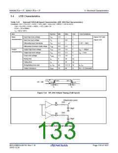
tLr
0.2
0.8
2.8
0.0
1.3
4
V
│ DP — DM │
2.5
3.6
0.3
2.0
20
V
Output
V
IOH = -200µA
IOL = 2mA
characteristics
V
V
Rising time
ns
ns
%
Ω
Falling time
tLf
4
20
Rising/falling time ratio
Output resistance
t
Lr / tLf
90
28
111.11
44
tLr / tLf
ZDRV
Rs = 22 Ωincluded
90%
90%
VCRS
DP、DM
10%
10%
tLr
tLf
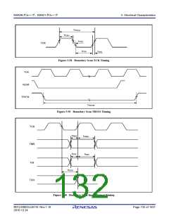
Figure 5.61 DP, DM Output Timing (Full-Speed)
Observation point
22Ω
dp
50pF
50pF
22Ω
dm
Figure 5.62 Test Circuit (Full-Speed)
R01UH0033JJ0110 Rev.1.10
2010.12.24
Page 133 of 1931

 RENESAS [ RENESAS TECHNOLOGY CORP ]