RX62Nグループ、RX621グループ
5. Electrical Characteristics
5.5
A/D Conversion Characteristics
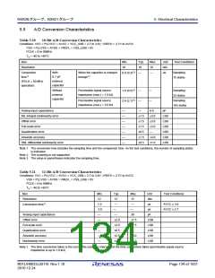
Table 5.20
10-Bit A/D Conversion Characteristics
Conditions: VCC = PLLVCC = AVCC = VCC_USB = 2.7 to 3.6V, VREFH = 2.7V to AVCC
VSS = PLLVSS = AVSS = VREFL = VSS_USB = 0V
PCLK = 8 to 50MHz
Ta = -40 to +85C
Item
Min.
Typ.
10
Max.
10
Unit
bits
µs
Test Conditions
Resolution
10
0.8 (0.3)*3
Conversion
time*1
With
When the capacitor is charged
enough*2
—
—
Sampling
15 states
0.1-µF
external
capacitor
(PCLK = 50-MHz
operation)
1.0 (0.5)*3
2.6 (2.1)*3
Without
external
capacitor
Permissible signal source
—
—
—
Sampling
25 states
Sampling
105 states
impedance (max.) = 1.0 kΩ
Permissible signal source
—
impedance (max.) = 5.0 kΩ
Analog input capacitance
INL integral nonlinearity error
Offset error
—
—
—
—
—
—
—
—
6.0
pF
±1.5
±1.5
±1.5
±0.5
±1.5
±0.5
±3.0
±3.0
±3.0
—
LSB
LSB
LSB
LSB
LSB
LSB
Full-scale error
Quantization error
Absolute accuracy
±3.0
±1.0
DNL differential nonlinearity error
Note 1. The conversion time includes the sampling time and the comparison time. As the test conditions, the number of sampling states
is indicated.
Note 2. The scanning is not supported.
Note 3. The value in parentheses indicates the sampling time.
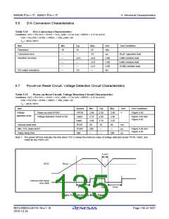
Table 5.21
12-Bit A/D Conversion Characteristics
Conditions: VCC = PLLVCC = AVCC = VCC_USB = 2.7 to 3.6V, VREFH = 2.7V to AVCC
VSS = PLLVSS = AVSS = VREFL = VSS_USB = 0V
PCLK = 8 to 50MHz
Ta = -40 to +85C
Item
Min.
12
1.0
2.0
—
Typ.
12
Max.
12
Unit
bits
µs
Test Conditions
Resolution
Conversion time*1
—
—
AVCC ≥ 3.0
AVCC ≥ 2.7
—
—
µs
Analog input capacitance
Offset error
—
30
pF
—
±2.0
±2.0
±0.5
±2.5
±2.0
±7.5
±7.5
—
LSB
LSB
LSB
LSB
LSB
Full-scale error
—
Quantization error
Absolute accuracy
Nonlinearity error
—
—
±8.0
±4.0
—
Note 1. The time conversion takes is the sum of the sampling interval and the time comparison takes (permissible signal-source
impedance is up to 1.0 kΩ)
R01UH0033JJ0110 Rev.1.10
2010.12.24
Page 134 of 1931

 RENESAS [ RENESAS TECHNOLOGY CORP ]