R8C/13 Group
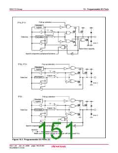
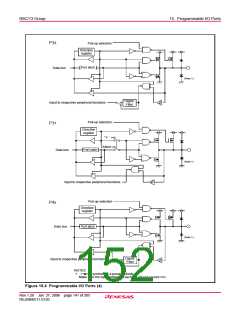
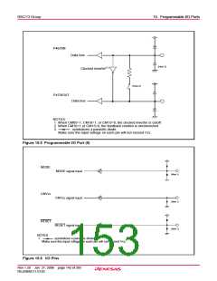
15. Programmable I/O Ports
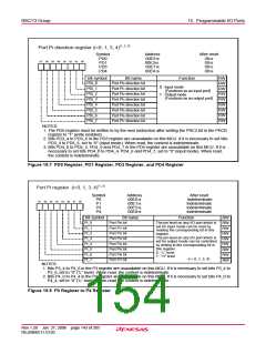
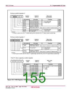
Pull-up control register 0
b7 b6 b5 b4 b3 b2 b1 b0
Symbol
PUR0
Address
00FC16
After reset
00XX0000
2
Bit symbol
PU00
Bit name
Function
RW
RW
RW
RW
RW
P0
P0
P1
P1
0
to P0
to P0
to P1
to P1
3
pull-up(1)
pull-up(1)
pull-up(1)
pull-up(1)
0 : Not pulled high
1 : Pulled high(1)
PU01
4
0
4
7
3
7
PU02
PU03
Nothing is assigned.
When write, set to “0”. When read, its content is indeterminate.
(b5-b4)
3
pull-up(1)
RW
RW
0 : Not pulled high
1 : Pulled high(1)
PU06
PU07
P3
0
to P3
pull-up(1)
P37
NOTES:
1. The pin for which this bit is “1” (pulled high) and the direction bit is “0” (input mode) is pulled high.
Pull-up control register 1
b7 b6 b5 b4 b3 b2 b1 b0
Symbol
PUR1
Address
00FD16
After reset
XXXXXX0X
2
Bit symbol
(b0)
Bit name
Function
RW
RW
Nothing is assigned.
When write, set to “0”. When read, its content is indeterminate.
P45
pull-up(1)
0 : Not pulled up
1 : Pulled up(1)
PU11
Nothing is assigned.
When write, set to “0”. When read, its content is indeterminate.
(b7-b2)
NOTES:
1. The P45 pin for which the PU11 bit is “1” (pulled high) and the PD4_5 bit is “0” (input mode) is pulled high.
Port P1 drive capacity control register
b7 b6 b5 b4 b3 b2 b1 b0
Symbol
DRR
Address
00FE16
After reset
0016
Bit symbol
Bit name
Function
RW
RW
RW
RW
DRR0
DRR1
DRR2
DRR3
DRR4
DRR5
DRR6
DRR7
P1
P1
P1
P1
P1
P1
P1
P1
0
1
2
3
4
5
6
7
drive capacity
drive capacity
drive capacity
drive capacity
drive capacity
drive capacity
drive capacity
drive capacity
Set P1 N-channel output transistor
drive capacity
0 : LOW
1 : HIGH
RW
RW
RW
RW
RW
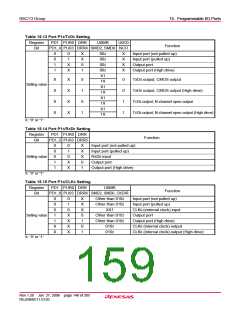
Figure 15.9 PUR0 Register, PUR1 Register, and DRR Register
Rev.1.20 Jan 27, 2006 page 144 of 205
REJ09B0111-0120

 RENESAS [ RENESAS TECHNOLOGY CORP ]