R8C/13 Group
15. Programmable I/O Ports
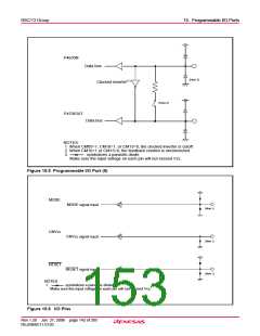
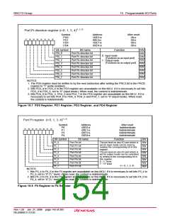
Port Pi direction register (i=0, 1, 3, 4)(1, 2, 3)
Symbol
PD0
PD1
PD3
PD4
Address
00E216
00E316
00E716
00EA16
After reset
0016
b7 b6 b5 b4 b3 b2 b1 b0
0016
0016
0016
Bit symbol
PDi_0
Bit name
Port Pi0 direction bit
Port Pi1 direction bit
Port Pi2 direction bit
Port Pi3 direction bit
Port Pi4 direction bit
Port Pi5 direction bit
Port Pi6 direction bit
Port Pi7 direction bit
Function
RW
RW
RW
RW
RW
RW
RW
RW
RW
0 : Input mode
(Functions as an input port)
1 : Output mode
PDi_1
PDi_2
(Functions as an output port)
PDi_3
PDi_4
PDi_5
PDi_6
PDi_7
NOTES:
1. The PD0 register must be written to by the next instruction after setting the PRC2 bit in the PRCR
register to “1” (write enabled).
2. Bits PD3_4 to PD3_6 in the PD3 register are unavailable on this MCU. If it is necessary to set bits
PD3_4 to PD3_6, set to “0” (input mode). When read, the content is indeterminate.
3. Bits PD4_0 to PD4_4, PD4_6 and PD4_7 in the PD4 register are unavailable on this MCU. If it is
necessary to set bits PD4_0 to PD4_4, PD4_6 and PD4_7, set to “0” (input mode). When read,
the content is indeterminate.
Figure 15.7 PD0 Register, PD1 Register, PD3 Register, and PD4 Register
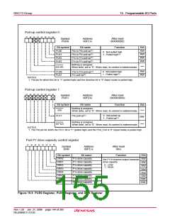
Port Pi register (i=0, 1, 3, 4)(1, 2)
Symbol
P0
P1
P3
P4
Address
00E016
00E116
00E516
00E816
After reset
Indeterminate
Indeterminate
Indeterminate
Indeterminate
b7 b6 b5 b4 b3 b2 b1 b0
Bit symbol
Pi_0
Bit name
Function
RW
RW
RW
RW
RW
RW
RW
RW
RW
The pin level on any I/O port which is
set for input mode can be read by
reading the corresponding bit in this
register.
The pin level on any I/O port which is
set for output mode can be controlled
by writing to the corresponding bit in
this register
Port Pi
Port Pi
Port Pi
Port Pi
Port Pi
Port Pi
Port Pi
Port Pi
0
1
2
3
4
5
6
7
bit
bit
bit
bit
bit
bit
bit
bit
Pi_1
Pi_2
Pi_3
Pi_4
Pi_5
0 : “L” level
1 : “H” level
Pi_6
(i = 0, 1, 3, 4)
Pi_7
NOTES:
1. Bits P3_4 to P3_6 in the P3 register are unavailable on this MCU. If it is necessary to set bits P3_4 to
P3_6, set to “0” (“L” level). When read, the content is indeterminate.
2. Bits P4_0 to P4_4 in the P4 register are unavailable on this MCU. If it is necessary to set bits P4_0 to
P4_4, set to “0” (“L” level). When read, the content is indeterminate.
Figure 15.8 P0 Register to P4 Register
Rev.1.20 Jan 27, 2006 page 143 of 205
REJ09B0111-0120

 RENESAS [ RENESAS TECHNOLOGY CORP ]