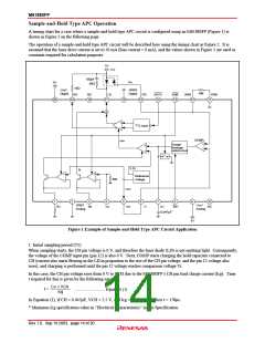
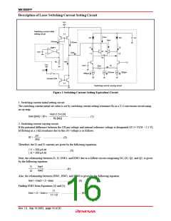
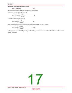
M61880FP
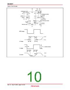
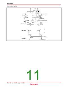
Sample-and-Hold Type APC Operation
A timing chart for a case where a sample-and-hold type APC circuit is configured using an M61880FP (Figure 1) is
shown in Figure 2 on the following page.
The operation of a sample-and-hold type APC circuit will be described here using the timing chart in Figure 2. It is
assumed that the laser drive current is set to 50 mA (bias current = 0 mA), and the values shown in Figure 1 are used as
constants required for calculation purposes.
5V
V
CC
100pF
I
PD
5V
20
36Ω
10Ω
Vcc2
Digital
GND2
Digital
RM
RO
19
NC
18
LD
PD
15
DATA
14
ENB
13
2RM
1RM
11
17
16
12
TTL input
COMP
I
SW
Charge/
discharge
control circuit
2.5V
I
B
Reference
voltage
50k
1.5V
1
2
3
4
5
6
7
8
9
10
GND1
Analog
Vcc1
Analog
RS
RB
V
B
V
ref
V
r
CH
S/H
NC
0.047µF
5V
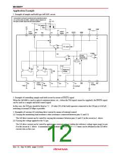
Figure 1 Example of Sample-and-Hold Type APC Circuit Application
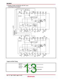
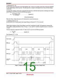
1. Initial sampling period (T1)
When sampling starts, the CH pin voltage is 0 V, and therefore the laser diode (LD) is not emitting light. Consequently,
the voltage of the COMP input pin (pin 12) is also 0 V. Next, COMP starts charging the hold capacitor connected to
CH (current also starts flowing in the LD in proportion to the rise of the CH pin voltage, and the pin 12 voltage also
rises), and charging is performed until the pin 12 voltage reaches comparison voltage Vr.
In this case, the CH pin voltage rises from 0 V to VCH due to the M61880FP’s CH pin load charge current (Icg). Time
t required for this is given by the following equation.
CH
× VCH
Icg
t =
............................ Equation (1)
In Equation (1), if CH = 0.047µF, VCH = 2.5 V, and Icg = 0.66 mA (*), then t = 178µs.
* Minimum Icg specification value in “Electrical Characteristics” in this Specification.
Rev.1.0, Sep.19.2003, page 14 of 20

 RENESAS [ RENESAS TECHNOLOGY CORP ]