3858 Group
Notes on Interrupts
Notes on Timer
• If a value n (between 0 and 255) is written to a timer latch, the
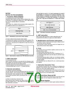
1. Change of relevant register settings
When the setting of the following registers or bits is changed, the
interrupt request bit may be set to “1”. When not requiring the in-
terrupt occurrence synchronized with these setting, take the
following sequence.
frequency division ratio is 1/(n+1).
• When switching the count source by the timer 12, X and Y count
source selection bits, the value of timer count is altered in
unconsiderable amount owing to generating of thin pulses in the
count input signals.
• Interrupt edge selection register (address 3A16)
• Timer XY mode register (address 2316)
Therefore, select the timer count source before set the value to
the prescaler and the timer.
Set the above listed registers or bits as the following sequence.
Notes on Serial Interface
Set the corresponding interrupt enable bit to “0” (disabled).
↓
1. Notes when selecting clock synchronous
Set the interrupt edge select bit (active edge switch bit) or
serial I/O (Serial I/O1)
(1) Stop of transmission operation
the interrupt (source) select bit to “1”.
↓
Clear the serial I/O1 enable bit and the transmit enable bit to “0”
(Serial I/O1 and transmit disabled).
NOP (one or more instructions)
↓
<Reason>
Set the corresponding interrupt request bit to “0”
(no interrupt request issued).
Since transmission is not stopped and the transmission circuit is
not initialized even if only the serial I/O1 enable bit is cleared to “0”
(Serial I/O1 disabled), the internal transmission is running (in this
case, since pins TxD, RxD, SCLK1, and SRDY1 function as I/O
ports, the transmission data is not output). When data is written to
the transmit buffer register in this state, data starts to be shifted to
the transmit shift register. When the serial I/O1 enable bit is set to
“1” at this time, the data during internally shifting is output to the
TxD pin and an operation failure occurs.
↓
Set the corresponding interrupt enable bit to “1” (enabled).
Fig 66. Sequence of changing relevant register
<Reason>
When setting the followings, the interrupt request bit may be set to
“1”.
• When setting external interrupt active edge
Concerned register: Interrupt edge selection register
(address 3A16)
(2) Stop of receive operation
Clear the receive enable bit to “0” (receive disabled), or clear the
serial I/O1 enable bit to “0” (Serial I/O1 disabled).
Timer XY mode register (address 2316)
• When switching interrupt sources of an interrupt vector address
where two or more interrupt sources are allocated.
Concerned register: Interrupt edge selection register
(address 3A16)
(3) Stop of transmit/receive operation
Clear the transmit enable bit and receive enable bit to “0” simulta-
neously (transmit and receive disabled).
(when data is transmitted and received in the clock synchronous
serial I/O mode, any one of data transmission and reception can-
not be stopped.)
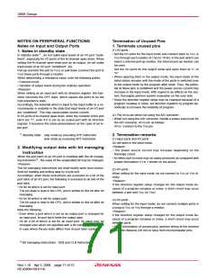
2. Check of interrupt request bit
When executing the BBC or BBS instruction to an interrupt re-
quest bit of an interrupt request register immediately after this bit
is set to “0” by using a data transfer instruction, execute one or
more instructions before executing the BBC or BBS instruction.
<Reason>
In the clock synchronous serial I/O mode, the same clock is used
for transmission and reception. If any one of transmission and re-
ception is disabled, a bit error occurs because transmission and
reception cannot be synchronized.
Clear the interrupt request bit to “0” (no interrupt issued)
In this mode, the clock circuit of the transmission circuit also oper-
ates for data reception. Accordingly, the transmission circuit does
not stop by clearing only the transmit enable bit to “0” (transmit
disabled). Also, the transmission circuit is not initialized by clear-
ing the serial I/O1 enable bit to “0” (Serial I/O1 disabled) (refer to
(1) in 1).
↓
NOP (one or more instructions)
↓
Execute the BBC or BBS instruction
*Data transfer instruction:
LDM, LDA, STA, STX, and STY instructions
(4) SRDY1 output of reception side (Serial I/O1)
Fig 67. Sequence of check of interrupt request bit
When signals are output from the SRDY1 pin on the reception side
by using an external clock in the clock synchronous serial I/O
mode, set all of the receive enable bit, the SRDY1 output enable
bit, and the transmit enable bit to “1” (transmit enabled).
<Reason>
If the BBC or BBS instruction is executed immediately after an in-
terrupt request bit of an interrupt request register is cleared to “0”,
the value of the interrupt request bit before being cleared to “0” is
read.
Rev.1.10 Apr 3, 2006 page 72 of 75
REJ03B0139-0110

 RENESAS [ RENESAS TECHNOLOGY CORP ]