3858 Group
NOTES ON PERIPHERAL FUNCTIONS
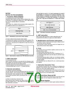
Notes on Input and Output Ports
1. Notes in standby state
Termination of Unused Pins
1. Terminate unused pins
(1) I/O ports :
• Set the I/O ports for the input mode and connect them to VCC or
VSS through each resistor of 1 kΩ to 10 kΩ. In the port which can
select a internal pull-up resistor, the internal pull-up resistor can
be used.
*1
In standby state , do not make input levels of an I/O port “unde-
fined”, especially for I/O ports of the N-channel open-drain. When
setting the N-channel open-drain port as an output, do not make
input levels of an I/O port “undefined”, too.
Set the I/O ports for the output mode and open them at “L” or
“H”.
Pull-up (connect the port to VCC) or pull-down (connect the port to
VSS) these ports through a resistor.
• When opening them in the output mode, the input mode of the
initial status remains until the mode of the ports is switched over
to the output mode by the program after reset. Thus, the poten-
tial at these pins is undefined and the power source current may
increase in the input mode. With regard to an effects on the sys-
tem, thoroughly perform system evaluation on the user side.
• Since the direction register setup may be changed because of a
program runaway or noise, set direction registers by program pe-
riodically to increase the reliability of program.
When determining a resistance value, note the following points:
• External circuit
• Variation of output levels during the ordinary operation
<Reason>
When setting as an input port with its direction register, the tran-
sistor becomes the OFF state, which causes the ports to be the
high-impedance state.
Accordingly, the potential which is input to the input buffer in a mi-
crocomputer is unstable in the state that input levels of an I/O port
are “undefined”. This may cause power source current.
In I/O ports of N-channel open-drain, when the contents of the port
latch are “1”, even if it is set as an output port with its direction
register, it becomes the same phenomenon as the case of an in-
put port.
(2) The AVSS pin when not using the A/D converter :
• When not using the A/D converter, handle a power source pin for
the A/D converter, AVSS pin as follows:
AVSS: Connect to the VSS pin.
*1
Standby state : stop mode by executing STP instruction
2. Termination remarks
(1) Input ports and I/O ports :
wait mode by executing WIT instruction
Do not open in the input mode.
<Reason>
2. Modifying output data with bit managing
• The power source current may increase depending on the
firststage circuit.
instruction
When the port latch of an I/O port is modified with the bit manag-
• An effect due to noise may be easily produced as compared with
proper termination (1) in 1 shown on the above.
*2
ing instruction , the value of the unspecified bit may be changed.
<Reason>
The bit managing instructions are read-modify-write form instruc-
tions for reading and writing data by a byte unit.
Accordingly, when these instructions are executed on a bit of the
port latch of an I/O port, the following is executed to all bits of the
port latch.
(2) I/O ports :
When setting for the input mode, do not connect to VCC or VSS di-
rectly.
<Reason>
If the direction register setup changes for the output mode be-
cause of a program runaway or noise, a short circuit may occur
between a port and VCC (or VSS).
• As for bit which is set for input port:
The pin state is read in the CPU, and is written to this bit after bit
managing.
• As for bit which is set for output port:
(3) I/O ports :
The bit value is read in the CPU, and is written to this bit after bit
managing.
When setting for the input mode, do not connect multiple ports in
a lump to VCC or VSS through a resistor.
Note the following:
<Reason>
• Even when a port which is set as an output port is changed for
an input port, its port latch holds the output data.
• As for a bit of which is set for an input port, its value may be
changed even when not specified with a bit managing instruction
in case where the pin state differs from its port latch contents.
If the direction register setup changes for the output mode be-
cause of a program runaway or noise, a short circuit may occur
between ports.
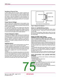
• At the termination of unused pins, perform wiring at the shortest
possible distance (20 mm or less) from microcomputer pins.
*2
Bit managing instructions : SEB and CLB instructions
Rev.1.10 Apr 3, 2006 page 71 of 75
REJ03B0139-0110

 RENESAS [ RENESAS TECHNOLOGY CORP ]