3858 Group
Notes on A/D Converter
Notes on Using Stop Mode
1. Analog input pin
1. Register setting
Make the signal source impedance for analog input low, or equip
an analog input pin with an external capacitor of 0.01 µF to 1 µF.
Further, be sure to verify the operation of application products on
the user side.
Since values of the prescaler 12 and Timer 1 are automatically re-
loaded when returning from the stop mode, set them again,
respectively. (When the oscillation stabilizing time set after STP in-
struction released bit is “0”)
<Reason>
When using the oscillation stabilizing time set after STP instruction
released bit set to “1”, evaluate time to stabilize oscillation of the
used oscillator and set the value to the timer 1 and prescaler 12.
An analog input pin includes the capacitor for analog voltage com-
parison. Accordingly, when signals from signal source with high
impedance are input to an analog input pin, charge and discharge
noise generates. This may cause the A/D conversion precision to
be worse.
2. Clock restoration
After restoration from the stop mode to the normal mode by an in-
terrupt request, the contents of the CPU mode register previous to
the STP instruction execution are retained. Accordingly, if both
main clock and sub clock were oscillating before execution of the
STP instruction, the oscillation of both clocks is resumed at resto-
ration.
2. A/D converter power source pin
The AVSS pin is A/D converter power source pin. Regardless of
using the A/D conversion function or not, connect it as following :
•AVSS : Connect to the VSS line
<Reason>
In the above case, when the main clock side is set as a system
clock, the oscillation stabilizing time for approximately 8,000
cycles of the XIN input is reserved at restoration from the stop
mode. At this time, note that the oscillation on the sub clock side
may not be stabilized even after the lapse of the oscillation stabi-
lizing time of the main clock side.
If the AVSS pin is opened, the microcomputer may have a failure
because of noise or others.
3. Clock frequency during A/D conversion
The comparator consists of a capacity coupling, and a charge of
the capacity will be lost if the clock frequency is too low. Thus,
make sure the following during an A/D conversion.
• f(XIN) is 500 kHz or more in middle-/high-speed mode.
• Do not execute the STP instruction.
• When the A/D converter is operated at low-speed mode, f(XIN)
do not have the lower limit of frequency, because of the A/D con-
verter has a built-in self-oscillation circuit.
Notes on Wait Mode
• Clock restoration
If the wait mode is released by a reset when XCIN is set as the
system clock and XIN oscillation is stopped during execution of the
WIT instruction, XCIN oscillation stops, XIN oscillations starts, and
XIN is set as the system clock.
In the above case, the RESET pin should be held at “L” until the
oscillation is stabilized.
Notes on Watchdog Timer
• Make sure that the watchdog timer does not underflow while
waiting Stop release, because the watchdog timer keeps count-
ing during that term.
Notes on Restarting Oscillation
• Restarting oscillation
• When the STP instruction disable bit has been set to “1”, it is im-
possible to switch it to “0” by a program.
Usually, when the MCU stops the clock oscillation by STP instruc-
tion and the STP instruction has been released by an external
interrupt source, the fixed values of Timer 1 and Prescaler 12
(Timer 1 = “0116”, Prescaler 12 = “FF16”) are automatically re-
loaded in order for the oscillation to stabilize.
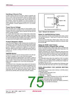
Notes on _R__E___S__E__T__ Pin
1. Connecting capacitor
____________
The user can inhibit the automatic setting by writing “1” to bit 0 of
MISRG (address 003816).
In case where the RESET signal rise time is long, connect a ce-
____________
ramic capacitor or others across the RESET pin and the VSS pin.
Use a 1000 pF or more capacitor for high frequency use. When
connecting the capacitor, note the following :
• Make the length of the wiring which is connected to a capacitor
as short as possible.
• Be sure to verify the operation of application products on the
user side.
<Reason>
However, by setting this bit to “1”, the previous values, set just be-
fore the STP instruction was executed, will remain in Timer 1 and
Prescaler 12. Therefore, you will need to set an appropriate value
to each register, in accordance with the oscillation stabilizing time,
before executing the STP instruction.
<Reason>
Oscillation will restart when an external interrupt is received.
However, internal clock φ is supplied to the CPU only when Timer
1 starts to underflow. This ensures time for the clock oscillation us-
ing the ceramic resonators to be stabilized.
If the several nanosecond or several ten nanosecond impulse
____________
noise enters the RESET pin, it may cause a microcomputer failure.
2. Reset release after power on
When releasing the reset after power on, such as power-on reset,
release reset after XIN passes more than 20 cycles in the state
where the power supply voltage is 2.7 V or more and the XIN os-
cillation is stable.
<Reason>
____________
To release reset, the RESET pin must be held at an “L” level for 20
cycles or more of XIN in the state where the power source voltage
is between 2.7 V and 5.5 V, and XIN oscillation is stable.
Rev.1.10 Apr 3, 2006 page 74 of 75
REJ03B0139-0110

 RENESAS [ RENESAS TECHNOLOGY CORP ]