3858 Group
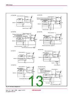
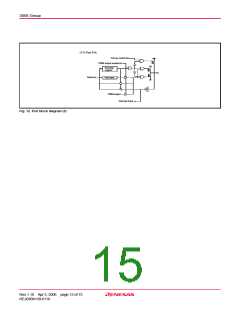
(2) Port P0
1
(1) Port P0
0
Pull-up control bit
Pull-up control bit
1/SOUT2 P-channel output disable bit
P0
Direction
register
Serial I/O2 Transmit completion signal
Serial I/O2 port selection bit
Direction
register
Port latch
Data bus
Data bus
Port latch
Serial I/O2 input
Pull-up control bit
Serial I/O2 output
(3) Port P0
2
(4) Port P03
Pull-up control bit
P02
/SCLK2 P-channel output disable bit
Serial I/O2 synchronous
clock selection bit
S
RDY2 output enable bit
Serial I/O2 port selection bit
Direction
register
Direction
register
Data bus
Port latch
Port latch
Data bus
Serial I/O2 ready output
Serial I/O2 clock output
Serial I/O2 external clock input
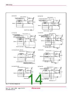
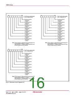
(6) Port P2
0
(5) Port P1
Pull-up control bit
Port X switch bit
Pull-up control bit
C
Direction
register
Direction
register
Port latch
Data bus
Data bus
Port latch
Oscillator
Port P2
1
Port XC switch bit
(7) Port P2
1
Pull-up control bit
(8) Ports P22,P2
3
Port X
C
switch bit
Timer Z operating
mode bits
Pull-up control bit
Direction
register
Bit 2
Bit 1
Bit 0
Data bus
Port latch
Direction
register
Data bus
Port latch
Sub-clock generating circuit input
Timer output
CNTR interrupt input
Fig. 10 Port block diagram (1)
Rev.1.10 Apr 3, 2006 page 13 of 75
REJ03B0139-0110

 RENESAS [ RENESAS TECHNOLOGY CORP ]