3858 Group
I/O PORTS
By setting the port P0 pull-up control register (address 001016),
the port P1 pull-up control register (address 001116), the port P2
pull-up control register (address 001216), the port P3 pull-up con-
trol register (address 001316), or the port P4 pull-up control
register (address 001416), ports can control pull-up with a pro-
gram. However, the contents of these registers do not affect ports
programmed as the output ports.
The I/O ports have direction registers which determine the input/
output direction of each individual pin. Each bit in a direction
register corresponds to one pin, and each pin can be set to be
input port or output port.
When “0” is written to the bit corresponding to a pin, that pin
becomes an input pin. When “1” is written to that bit, that pin
becomes an output pin.
If data is read from a pin which is set to output, the value of the
port output latch is read, not the value of the pin itself. Pins set to
input are floating. If a pin set to input is written to, only the port
output latch is written to and the pin remains floating.
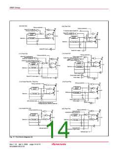
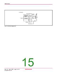
Table 5 I/O port function
Input/Output
Input/output, CMOS compatible
Related SFRs
Name
I/O Structure
Non-Port Function
Ref.No.
Pin
P00/SIN2
P01/SOUT2
P02/SCLK2
P03/SRDY2
Port P0
Serial I/O2 function I/O
Serial I/O2 control register
(1)
(2)
(3)
(4)
individual
bits
input level
CMOS 3-state output
P04/AN5–P07AN8
A/D converter input
AD control register
(13)
AD input selection register
Port P1
Port P2
P10–P17
(5)
P20/XCOUT
P21/XCIN
Sub-clock generating CPU mode register
circuit
(6)
(7)
P22/CNTR2
P23/CNTR3
Timer Z1 function I/O
Timer Z2 function I/O
Timer Z1 mode register
Timer Z2 mode register
(8)
(8)
P24/RxD
P25/TxD
P26/SCLK1
Serial I/O1 function I/O Serial I/O1 control register
(9)
(10)
(11)
P27/CNTR0/SRDY1
Timer X function I/O Timer XY mode register
(12)
Serial I/O1 function I/O
A/D converter input
Serial I/O1 control register
Port P3
(Note)
P30/AN0–
P34/AN4
AD control register
AD input selection register
(13)
Port P4
(Note)
P40/CNTR1
Timer Y function I/O
Timer XY mode register
(14)
(15)
P41/INT0
P42/INT1
External interrupt input Interrupt edge selection
register
P43/INT2/SCMP2
External interrupt input
SCMP2 output
Interrupt edge selection
register
Serial I/O2 control register
(16)
(17)
P44/INT3/PWM
External interrupt input Interrupt edge selection
PWM output
register
PWM control register
Note: When bits 5 to 7 of Ports P3 and P4 are read out, the contents are undefined.
Rev.1.10 Apr 3, 2006 page 12 of 75
REJ03B0139-0110

 RENESAS [ RENESAS TECHNOLOGY CORP ]