MITSUBISHI MICROCOMPUTERS
M37754M8C-XXXGP, M37754M8C-XXXHP
M37754S4CGP, M37754S4CHP
SINGLE-CHIP 16-BIT CMOS MICROCOMPUTER
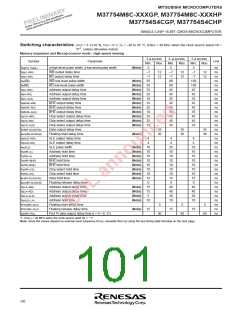
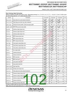
Timing requirements (VCC = 5 V±10 %, VSS = 0 V, Ta = –20 to 85 °C, f(XIN)=40 MHz when the clock source select bit = “0” , unless
otherwise noted)
✽ The rise and fall time of input signal must be 100 ns or less respectively, unless otherwise noted.
Memory expansion and Microprocessor mode : High-speed running
Limits
Symbol
Parameter
External clock input cycle time (Note 1)
Unit
Min.
25
Max.
tc
ns
ns
ns
ns
ns
ns
ns
ns
ns
ns
ns
tw(H)
External clock input high-level pulse width (Note 2)
External clock input low-level pulse width (Note 2)
External clock rise time
tc/2 – 8
tc/2 – 8
tw(L)
tr
8
8
tf
External clock fall time
tsu(DH–RD)
tsu(DL–RD)
tsu(PiD–RD)
th(RD–DH)
th(RD–DL)
th(RD–PiD)
High-order data input setup time (BYTE = “L”)
Low-order data input setup time
30
30
60
0
Port Pi input setup time (i = 4—9, 11)
High-order data input hold time (BYTE = “L”)
Low-order data input hold time
0
Port Pi input hold time (i = 4—9, 11)
0
65 (3-φ access)
110 (4-φ access)
160 (5-φ access)
65 (3-φ access)
110 (4-φ access)
160 (5-φ access)
50 (3-φ access)
100 (4-φ access)
150 (5-φ access)
tsu(A–DL/DH)
tsu(CS–DL/DH)
tsu(LA–DL)
Data setup time with address stabilized (Note 3)
Data setup time with chip select stabilized (Note 3)
Data setup time with address stabilized (Note 3)
ns
ns
ns
: f(XIN) = 20 MHz when the clock source selet bit = “1”
Notes 1: When the clock source select bit = “1”, tc’s minimum limit is 50 ns.
2: When the clock source select bit = “1”, set tw(H)/tc and tw(L)/tc ratios to 45 to 55 %.
3: Since the values depend on external clock input frequency f(XIN), calculate them using the bus timing data formula on the page after
the next page.
99

 RENESAS [ RENESAS TECHNOLOGY CORP ]