MITSUBISHI MICROCOMPUTERS
M37754M8C-XXXGP, M37754M8C-XXXHP
M37754S4CGP, M37754S4CHP
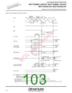
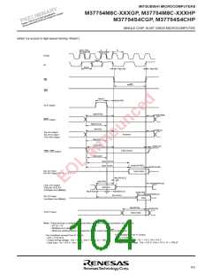
SINGLE-CHIP 16-BIT CMOS MICROCOMPUTER
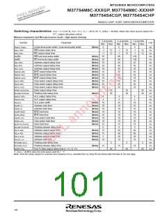
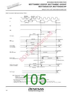
Bus timing data formulas
Memory expansion and Microprocessor mode : High-speed running (VCC = 5 V±10 %, VSS = 0 V, Ta = –20 to 85 °C, f(XIN) ≤ 40 MHz when
the clock source select bit = “0” , unless otherwise noted)
Symbol
tsu(A–DL/DH)
tsu(CS–DL/DH)
tw(φH), tw(φL)
Parameter
Data setup time with address stabilized
Data setup time with chip select stabilized
3-φ access
5 × 10⁹
4-φ access
7 × 10⁹
5-φ access
9 × 10⁹
Unit
ns
ns
ns
ns
ns
ns
ns
ns
ns
ns
ns
ns
ns
ns
ns
ns
ns
ns
ns
ns
ns
ns
ns
ns
ns
ns
ns
ns
– 60
– 65
– 65
f(XIN)
f(XIN)
f(XIN)
5 × 10⁹
f(XIN)
1 × 10⁹
f(XIN)
3 × 10⁹
f(XIN)
2 × 10⁹
f(XIN)
2 × 10⁹
f(XIN)
1 × 10⁹
f(XIN)
2 × 10⁹
f(XIN)
2 × 10⁹
f(XIN)
1 × 10⁹
f(XIN)
2 × 10⁹
f(XIN)
2 × 10⁹
f(XIN)
1 × 10⁹
f(XIN)
1 × 10⁹
f(XIN)
1 × 10⁹
f(XIN)
1 × 10⁹
f(XIN)
1 × 10⁹
f(XIN)
7 × 10⁹
f(XIN)
9 × 10⁹
f(XIN)
– 60
– 20
– 20
– 25
– 25
– 15
– 25
– 25
– 15
– 25
– 25
– 15
– 15
– 15
– 15
– 15
– 15
– 15
– 15
– 10
+ 5
– 65
– 65
φ high-level pulse width, φ low-level pulse width
4 × 10⁹
f(XIN)
3 × 10⁹
f(XIN)
3 × 10⁹
f(XIN)
2 × 10⁹
f(XIN)
3 × 10⁹
f(XIN)
3 × 10⁹
f(XIN)
2 × 10⁹
f(XIN)
3 × 10⁹
f(XIN)
6 × 10⁹
f(XIN)
___ ___
__
__
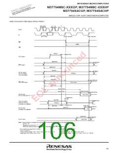
tw(WR), tw(RD) WR, RD low-level pulse width
– 20
– 30
– 30
– 15
– 30
– 30
– 15
– 30
– 30
– 15
– 15
– 20
td(A–WR)
Address output delay time
Address output delay time
Address output delay time
td(A–RD)
td(A–ALE)
td(BHE–WR)
td(BHE–RD)
td(BHE–ALE)
td(CS–WR)
td(CS–RD)
td(CS–ALE)
tw(ALE)
____
BHE outuput delay time
____
BHE outuput delay time
____
BHE outuput delay time
Chip select output delay time
Chip select output delay time
Chip select output delay time
ALE pulse width
3 × 10⁹
f(XIN)
2 × 10⁹
f(XIN)
2 × 10⁹
f(XIN)
th(WR–A)
Address hold time
th(RD–A)
Address hold time
____
td(WR–BHE)
td(RD–BHE)
td(WR–CS)
td(RD–CS)
BHE hold time
1 × 10⁹
f(XIN)
1 × 10⁹
f(XIN)
1 × 10⁹
f(XIN)
1 × 10⁹
f(XIN)
____
BHE hold time
Chip select hold time
Chip select hold time
t
h(WR–DLQ/DHQ)
Data hold time
1 × 10⁹
f(XIN)
tpxz(WR–DLZ/DHZ)
Floating start delay time
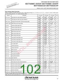
Data setup time with address stabilized
Address outuput delay time
Address outuput delay time
Address outuput delay time
Address hold time
5 × 10⁹
f(XIN)
2 × 10⁹
f(XIN)
2 × 10⁹
f(XIN)
1 × 10⁹
f(XIN)
1 × 10⁹
f(XIN)
1 × 10⁹
f(XIN)
7 × 10⁹
f(XIN)
3 × 10⁹
f(XIN)
3 × 10⁹
f(XIN)
2 × 10⁹
f(XIN)
9 × 10⁹
f(XIN)
tsu(LA–DL)
td(LA–WR)
td(LA–RD)
– 75
– 35
– 35
– 20
– 15
– 10
– 75
– 35
– 35
– 20
– 75
td(LA–ALE)
td(ALE–LA)
tpzx(RD–DLZ)
Floating release delay time
✽: f(XIN) ≤ 20 MHz when the clock source select bit = “1”
Note: When the clock source select bit is “1”, regard f(XIN) in tables as 2·f(XIN).
101

 RENESAS [ RENESAS TECHNOLOGY CORP ]