M37161M8/MA/MF-XXXSP/FP,M37161EFSP/FP
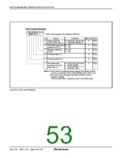
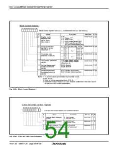
Block Control register i
b7 b6 b5b4 b3 b2b1 b0
Block control register i (BCi) (i=1, 2) [Addresses 00D216 and 00D316
]
After reset
B
Name
Functions
R W
R W
b1 b0
Indeterminate
0, 1 Display mode
selection bits
(BCi0, BCi1)
0
0
1
1
0: Display OFF
1: OSD1 mode
0: OSD2 mode (Border OFF)
1: OSD2 mode (Border ON)
/CD OSD mode (Border OFF)
(See note 4)
b4 b3 b2 Pre-divide Ratio Dot Size
Indeterminate
Indeterminate
2, 3 Dot size selection
bits (BCi2, BCi3)
(See note 1)
R W
R W
0
0
1
1
0
0
1
1
0
1
0
1
0
1
0
1
1Tc ✕ 1/2H
1Tc ✕ 1H
2Tc ✕ 2H
3Tc ✕ 3H
1Tc ✕ 1/2H
1Tc ✕ 1H
2Tc ✕ 2H
3Tc ✕ 3H
0
1
✕ 2
4
Pre-divide ratio
selection bit (BCi4)
✕ 3
0: 2 value output control
1: 3 value output control
(See note 3)
5
6
OUToutput control bit
(BCi5)
Indeterminate
Indeterminate
R W
R W
Vertical display start
position control bit
(BCi6)
BC16: Block 1
BC26: Block 1
BC17: Window top boundary
BC27: Window bottom boundary
Indeterminate
7
Window top/bottom
boundary control bit
(BCi7)
R W
Notes 1: Tc is OSD clock cycle divided in pre-divide circuit.
2: H is HSYNC
3: Refer to the corresponding figure 8.10.18.
.
4: Selection in OSD2 mode / CD OSD mode is performed in the bits 0 and 1
of color dot OSD control registration.
Fig. 8.10.4 Block Control Register i
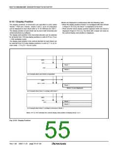
Color dot OSD control register
b7 b6 b5 b4 b3 b2 b1 b0
Color dot OSD control register (CDT) [Address 00DA16
]
R
R
B
0
Name
Functions
0 : OSD2 mode
After reset
W
W
Indeterminate
Color dot Block 1 Setting bit
(CDT0)
1 : CD OSD mode
1
Color dot Block 2 Setting bit
(CDT1)
0 : OSD2 mode
1 : CD OSD mode
Indeterminate
Indeterminate
R
R
W
—
2
to
7
Nothing is assigned. This bit is write disable bit.
When this bit is read out, the value is "Indeterminate."
Fig. 8.10.5 Color dot OSD Control Register
Rev.1.00 2003.11.25 page 54 of 128

 RENESAS [ RENESAS TECHNOLOGY CORP ]