M37161M8/MA/MF-XXXSP/FP,M37161EFSP/FP
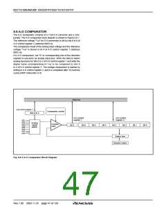
8.8 A-D COMPARATOR
The A-D comparator consists of a 7-bit D-A converter and a com-
parator. The A-D comparator block diagram is shown in Figure 8.8.1.
The reference voltage “Vref” for D-A conversion is set by bits 0 to 6 of
A-D control register 2 (address 00ED16).
The comparison result of the analog input voltage and the reference
voltage “Vref” is stored in bit 4 of A-D control register 1 (address
00EC16).
For A-D comparison, set “0” to corresponding bits of the direction
register to use ports as analog input pins. Write the data to select
analog input pins for bits 0 to 2 of A-D control register 1 and write the
digital value corresponding to Vref to be compared to bits 0
to 4 of A-D control register 2. The voltage comparison is started by
writing to A-D control register 2, and it is completed after 16 machine
cycles (NOP instruction ✕✕8).
Data bus
A-D control register 1
Comparator control
Bits 0 to 2
A-D control
register 1
A-D control
register 2
AD1
AD2
AD3
AD4
AD5
AD6
Analog
signal
switch
Compa-
rator
Bit 4
Bit 6
Bit 5
Bit 4
Bit 3
Bit 2
Bit 1
Bit 0
AD7
AD8
Switch tree
Resistor ladder
Fig. 8.8.1 A-D Comparator Block Diagram
Rev.1.00 2003.11.25 page 47 of 128

 RENESAS [ RENESAS TECHNOLOGY CORP ]