M37161M8/MA/MF-XXXSP/FP,M37161EFSP/FP
8.9 ROM CORRECTION FUNCTION
This can correct program data in the ROM. Up to 2 addresses can be
corrected; a program for correction is stored in the ROM correction
vector in the RAM as the top address. There are 2 vectors for ROM
correction :
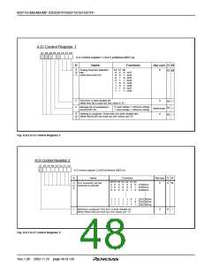
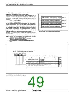
ROM correction address 1 (high-order) 020A16
ROM correction address 1 (low-order) 020B16
ROM correction address 2 (high-order) 020C16
Vector 1 : address 030016
Vector 2 : address 032016
Set the address of the ROM data to be corrected into the ROM cor-
rection address register. When the value of the counter matches the
ROM data address in the top address of the ROM correction vector,
the main program branches to the correction program stored in the
ROM memory. To return from the correction program to the main
program, the op code and operand of the JMP instruction (total of 3
bytes) are necessary at the end of the correction program.
The ROM correction function is controlled by the ROM correction
enable register.
ROM correction address 2 (low-order)
020D16
Fig. 8.9.1 ROM Correction Address Registers
Notes 1: Specify the first address (op code address) of each
instruction as the ROM correction address.
2: Use the JMP instruction (total of 3 bytes) to return from
the correction program to the main program.
3: Do not set the same ROM correction address to both vectors 1
and 2.
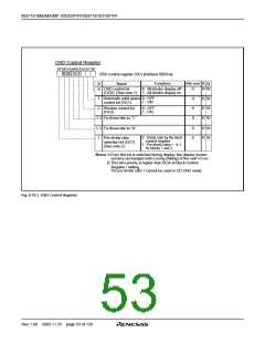
ROM Correction Enable Register
b7 b6 b5 b4 b3 b2 b1 b0
ROM correction enable register (RCR) [Address 020E 16
]
After reset
0
B
Name
Functions
R W
R W
0
Vector 1 enable bit (RC0)
0: Disabled
1: Enabled
1
Vector 2 enable bit (RC1)
0: Disabled
1: Enabled
0
0
R W
Nothing is assigned. These bits are write disable bits. When
these bits are read out, the values are “0.”
2
to
7
R —
Fig. 8.9.2 ROM Correction Enable Register
Rev.1.00 2003.11.25 page 49 of 128

 RENESAS [ RENESAS TECHNOLOGY CORP ]