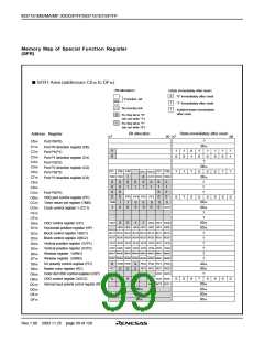
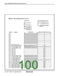
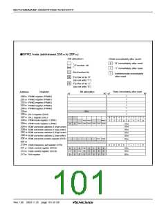
M37161M8/MA/MF-XXXSP/FP,M37161EFSP/FP
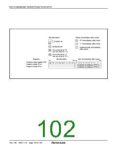
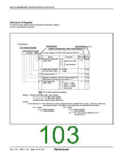
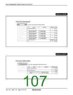
Structure of Register
The figure of each register structure describes its functions, contents
at reset, and attributes as follows:
<Example>
Bit position
Bit attributes(Note 2)
CPU Mode Register
(Note 1)
Values immediately after reset release
b7b6 b5b4b3 b2b1b0
1 1 0 0
CPU mode register (CPUM) (CM) [Address 00FB16
]
B
Name
Functions
After reset R W
Processor mode bits b1 b0
0, 1
0
R W
(CM0, CM1)
0 0: Single-chip mode
0 1:
1 0:
1 1:
Not available
0: 0 page
1: 1 page
Stack page selection
bit (See note) (CM2)
2
1
R W
3, 4 Fix these bits to “1.”
1
1
R W
R W
5
Nothing is assigned. This bit is write disable bit.
When this bit is read out, the value is “1.”
Clock switch bits
(CM6, CM7)
b7 b6
6, 7
0
R W
0
0
1
1
0: f(XIN) = 8 MHz
1: f(XIN) = 12 MHz
0: f(XIN) = 16 MHz
1: Do not set
: Bit in which nothing is assigned
Notes 1: Values immediately after reset release
0 ••••••••••••••••••“0” after reset release
1 ••••••••••••••••••“1” after reset release
Indeterminate•••Indeterminate after reset
release
2: Bit attributes••••••The attributes of control register bits are classified into 3 types : read-only, write-only
and read and write. In the figure, these attributes are represented as follows :
R••••••Read
W••••••Write
W
R
••••••Read enabled
••••••Read disabled
••••••Write enabled
–
–
••••••Write disabled
ꢀ ••••••“0” can be set by software, but “1”
cannot be set.
Rev.1.00 2003.11.25 page 103 of 128

 RENESAS [ RENESAS TECHNOLOGY CORP ]