4283 Group
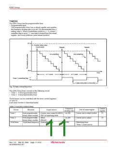
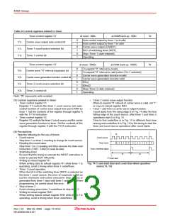
Table 4 Control registers related to timer
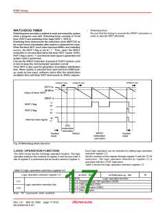
Timer control register V1
at reset : 0002
at RAM back-up : 0002
W
0
1
0
1
0
1
Auto-control output by timer 1 is invalid
Auto-control output by timer 1 is valid
Carrier wave output (CARRY)
Bit 5 of watchdog timer (WDT)
Stop (Timer 1 state retained)
Operating
V12
V11
V10
Carrier wave output auto-control bit
Timer 1 count source selection bit
Timer 1 control bit
Timer control register V2
at reset : 00002
at RAM back-up : 00002
W
0
1
0
1
0
1
0
1
To expand “H” interval is invalid
To expand “H” interval is valid (when V22=1 selected)
Carrier wave generation function invalid
Carrier wave generation function valid
f(XIN)
V23
V22
V21
V20
Carrier wave “H” interval expansion bit
Carrier wave generation function control bit
Timer 2 count source selection bit
Timer 2 control bit
f(XIN)/2
Stop (Timer 2 state retained)
Operating
Note: “W” represents write enabled.
(1) Control registers related to timer
•
•
Timer 2 carrier wave output function
When to expand “H” interval of carrier wave is valid, set “1”
or more to reload register R2H.
•
Timer control register V1
Register V1 controls the timer 1 count source and auto-
control function of carrier wave output from port CARR by
timer 1. Set the contents of this register through register A
with the TV1A instruction.
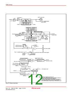
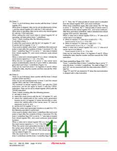
Timer 1 and timer 2 carrier wave output function
Count starts from the rising edge in Fig. 14 after the first
➁
falling edge of the count source, after timer 1 and timer 2
•
Timer control register V2
operations start in Fig. 14.
➁
Register V2 controls the timer 2 count source and the carrier
wave generation function by timer. Set the contents of this
register through register A with the TV2A instruction.
Time to first underflow in Fig. 14 is different from time
➁
among next underflow in Fig. 14 by the timing to start the
➁
timer and count source operations after count starts.
(2) Precautions
➁
Note the following for the use of timers.
•
•
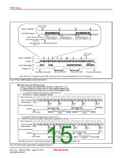
Count source
Count source
Stop timer 1 or timer 2 counting to change its count source.
Reading the count value
Timer value
3
2
1
0
3
2
1
0
3
Stop timer 1 or 2 counting and then execute the data read
instruction (TAB1, TAB2) to read its data.
Watchdog timer
Be sure that the timing to execute the WRST instruction in
order to operate WDT efficiently.
Timer underflow signal
•
•
•
➁
➁
➁
Timer start
Writing to reload register R1
When writing data to reload register R1 while timer 1 is
operating, avoid a timing when timer 1 underflows.
Timer 1 count operation
Fig. 14 Count start time and count time when operation
starts (T1, T2)
When the bit 5 of the watchdog timer (WDT) is selected as
the timer 1 count source, the error of maximum ± 256 µs
(at the minimum instruction execution time : 8 µs) is
generated from timer 1 start until timer 1 underflow. When
programming, be careful about this error.
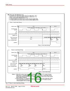
Stop of timer 2
•
•
Avoid a timing when timer 2 underflows to stop timer 2.
Writing to reload register R2H
When writing data to reload register R2H while timer 2 is
operating, avoid a timing when timer underflows.
Rev.1.01 Mar 20, 2006 page 13 of 62
REJ03B0109-0101

 RENESAS [ RENESAS TECHNOLOGY CORP ]