4283 Group
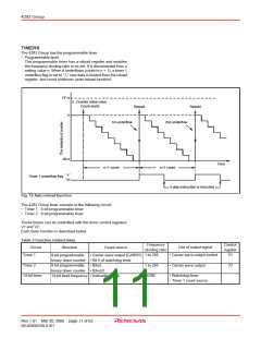
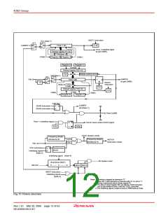
SNZT1 instruction
V10 (Note 1)
V1
0
1
0
Timer 1 (8)
CARRY
T1F
1
1
Timer 1 underflow signal
(to port CARR)
Reload register R1 (8)
(T1AB)
(Note 2)
(TAB1)
Register B Register A
(TAB1)
Register B
Register A
(T2HAB)
Reload register R2H (8)
Reload control circuit
V2
3
V20 (Note 1)
0
V2
1
0
CARRYD
X
IN
Timer 2(8)
T
Q
1
(to port CARR)
1
R
1/2
SNZT2
(T2R2L)
(T2AB)
instruction
(Note 3)
V2
2
Reload register R2L (8)
(T2AB)
T2F
T2F
(TAB2)
(TAB2)
Register B
Register A
CAR flag
CARRY
(to timer 1)
SCAR instruction
RCAR instruction
S
R
Q
Port CARR
Timer 1 underflow signal
D
T
Q
R
Carrier wave output control signal
V1
2
V10
STCK (System clock)
Frequency divider
(divided by 8)
Frequency divider
(divided by 4)
INSTCK
(Instruction clock)
XIN
CCK instruction
Synchronous
circuit
S
R
Q
Initializing signal
(Note 3)
Initializing signal
(Note 4)
System reset
14-bit timer (WDT)
INSTCK
0
5
13
WDF1 WDF2
WRST instruction
Initializing signal
(Note 4)
Notes 1: Counting is stopped by clearing to “0.”
2: When the T1AB instruction is executed after V1
writing is performed only to reload register R1.
0
is set to “1,”
3: The data of reload register R2L set with the T2AB instruction
can be also written to timer 2 with the T2R2L instruction.
4: The initializing signal is output at reset or RAM back-up mode.
Fig. 13 Timers structure
Rev.1.01 Mar 20, 2006 page 12 of 62
REJ03B0109-0101

 RENESAS [ RENESAS TECHNOLOGY CORP ]