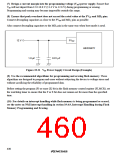
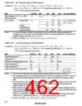
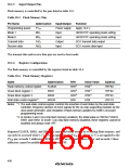
Table 19.18 DC Characteristics of Flash Memory
Conditions: VCC = 2.7 V to 5.5 V*2, AVCC = 2.7 V to 5.5 V*2,VSS = AVSS = 0 V,
VPP = 12.0 ± 0.6 V, Ta = –20°C to +75°C (regular specifications), Ta = –40°C to
+85°C (wide-range specifications)
Item
Symbol Min
Typ
Max
Unit Test Conditions
High-voltage (12 V) FVPP, MD1
threshold level*1
VH
VCC + 2
—
11.4
V
FVPP current
During read
IPP
—
—
—
—
10
20
10
20
40
µA
VPP = 2.7 to 5.5 V
VPP = 12.6 V
mA
mA
During
programming
During erasure
—
20
40
mA
Notes: *1 The listed voltages indicate the threshold level at which high-voltage application is
recognized. In boot mode and while flash memory is being programmed or erased, the
applied voltage should be 12.0 V ± 0.6 V.
*2 In the LH version, VCC = 3.0 V to 5.5 V, AVCC = 3.0 V to 5.5 V
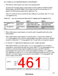
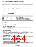
Table 19.19 AC Characteristics of Flash Memory
Conditions: VCC = 2.7 V to 5.5 V*5, AVCC = 2.7 V to 5.5 V*5, VSS = AVSS = 0 V,
VPP = 12.0 ± 0.6 V, Ta = –20°C to +75°C (regular specifications), Ta = –40°C to
+85°C (wide-range specifications)
Item
Symbol Min
Typ
50
1
Max
1000
30
Unit
µs
Test Conditions
Programming time*1, *2
Erase time*1, *3
tP
tE
—
—
—
4
s
Number of writing/erasing count NWEC
—
—
—
—
—
100
—
Times
µs
Verify setup time 1*1
Verify setup time 2*1
Flash memory read setup time*4 tFRS
tVS1
tVS2
2
—
µs
50
100
—
µs
VCC ≥ 4.5 V
—
VCC < 4.5 V
Notes: *1 Set the times following the programming/erasing algorithm shown in section 19.
*2 The programming time is the time during which a byte is programmed or the P bit in the
flash memory control register (FLMCR) is set. It does not include the program-verify
time.
*3 The erase time is the time during which all 32-kbyte blocks are erased or the E bit in the
flash memory control register (FLMCR) is set. It does not include the prewrite time
before erasure or erase-verify time.
*4 After power-on when using an external clock source, after return from standby mode, or
after switching the programming voltage (VPP) from 12 V to VCC, make sure that this read
setup time has elapsed before reading flash memory.
When VPP is released, the flash memory read setup time is defined as the period from
when the FVPP pin has reached VCC + 2 V until flash memory can be read.
*5 In the LH version, VCC = 3.0 V to 5.5 V, AVCC = 3.0 V to 5.5 V.
432

 RENESAS [ RENESAS TECHNOLOGY CORP ]