(7) Design a current margin into the programming voltage (VPP) power supply. Ensure that
VPP will not depart from 12.0 ±0.6 V (11.4 V to 12.6 V) during programming or erasing.
Programming and erasing may become impossible outside this range.
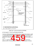
(8) Ensure that peak overshoot does not exceed the rated value at the FVPP and MD1 pins.
Connect decoupling capacitors as close to the FVPP and MD1 pins as possible.
Also connect decoupling capacitors to the MD1 pin in the same way when boot mode is uesd.
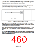
FVPP
12 V
H8/3334YF
1.0 µF
0.01 µF
Figure 19.21 VPP Power Supply Circuit Design (Example)
(9) Use the recommended algorithms for programming and erasing flash memory. These
algorithms are designed to program and erase without subjecting the device to voltage stress and
without sacrificing the reliability of programmed data.
Before setting the program (P) or erase (E) bit in the flash memory control register (FLMCR), set
the watchdog timer to ensure that the P or E bit does not remain set for more than the specified
time.
(10) For details on interrupt handling while flash memory is being programmed or erased,
see the notes on NMI interrupt handling in section 19.4.9, Interrupt Handling during Flash
Memory Programming and Erasing.
430

 RENESAS [ RENESAS TECHNOLOGY CORP ]