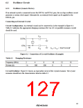
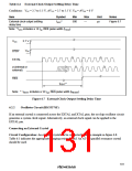
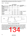
External Clock Input: The external clock signal should have the same frequency as the desired
system clock (ø). Clock timing parameters are given in table 6.3 and figure 6.6.
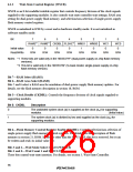
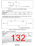
Table 6.3 Clock Timing
VCC = 2.7 to VCC = 4.0 to VCC = 5.0 V
5.5 V
5.5 V
±10%
Item
Symbol Min Max
Min Max
Min Max
Unit Test Conditions
Low pulse
tEXL
40
—
30
—
20
—
ns
Figure 6.6
width of external
clock input
High pulse
tEXH
40
—
30
—
20
—
ns
width of external
clock input
External clock
rise time
tEXr
tEXf
tCL
—
—
10
10
—
—
10
10
—
—
5
5
ns
ns
External clock
fall time
Clock pulse
width low
0.3
0.4
0.3
0.4
0.7
0.6
0.7
0.6
0.3
0.4
0.3
0.4
0.7
0.6
0.7
0.6
0.3
0.4
0.3
0.4
0.7
0.6
0.7
0.6
tcyc
tcyc
tcyc
tcyc
ø ≥ 5 MHz Figure
20-4
ø < 5 MHz
Clock pulse
width high
tCH
ø ≥ 5 MHz
ø < 5 MHz
tEXH
tEXL
EXTAL
VCC × 0.5
tEXr
tEXt
Figure 6.6 External Clock Input Timing
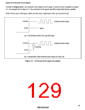
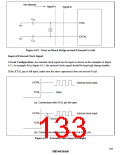
Table 6.4 shows the external clock output settling delay time. Figure 6.7 shows the timing for the
external clock output settling delay time. The oscillator and duty correction circuit have the
function of regulating the waveform of the external clock input to the EXTAL pin. When the
specified clock signal is input to the EXTAL pin, internal clock signal output is confirmed after
the elapse of the external clock output settling delay time (tDEXT). As clock signal output is not
confirmed during the tDEXT period, the reset signal should be driven low and the reset state
maintained during this time.
100

 RENESAS [ RENESAS TECHNOLOGY CORP ]