6.1.2
Wait-State Control Register (WSCR)
WSCR is an 8-bit readable/writable register that controls frequency division of the clock signals
supplied to the supporting modules. It also controls wait state controller wait settings, RAM area
setting for dual-power-supply flash memory, and selection/non-selection of single-power-supply
flash memory control registers.
WSCR is initialized to H'08 by a reset and in hardware standby mode. It is not initialized in
software standby mode.
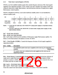
Bit
7
6
5
4
3
2
WMS0
0
1
0
RAMS*1 RAM0*1 CKDBL FLSHE*2 WMS1
WC1
0
WC0
0
Initial value
Read/Write
0
0
0
0
1
R/W
R/W
R/W
R/W
R/W
R/W
R/W
R/W
Notes: *1 These bits are valid only in the H8/3337YF (dual-power-supply on-chip flash memory
versions).
*2 This bit is valid only in the H8/3337SF (S-mask model, single-power-supply on-chip
flash memory version).
Bit 7—RAM Select (RAMS)
Bit 6—RAM Area Select (RAM0)
Bits 7 and 6 select a RAM area for emulation of dual-power-supply flash memory updates. For
details, see the flash memory description in section 18, ROM.
Bit 5—Clock Double (CKDBL): Controls the frequency division of clock signals supplied to
supporting modules.
Bit 5: CKDBL
Description
0
The undivided system clock (ø) is supplied as the clock (øP) for supporting
modules.
(Initial value)
1
The system clock (ø) is divided by two and supplied as the clock (øP) for
supporting modules.
Bit 4—Flash Memory Control Register Enable (FLSHE): Controls selection/non-selection of
single-power-supply flash memory control registers. For details, see the description of flash
memory in section 21, ROM. In models other than the H8/3337SF, this bit is reserved, but it can
be written and read; its initial value is 0.
Bits 3 and 2—Wait Mode Select 1 and 0 (WMS1/0)
Bits 1 and 0—Wait Count 1 and 0 (WC1/0)
These bits control wait-state insertion. For details, see section 5, Wait-State Controller.
96

 RENESAS [ RENESAS TECHNOLOGY CORP ]