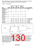
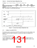
Table 6.4 External Clock Output Settling Delay Time
Conditions: VCC = 2.7 to 5.5 V, AVCC = 2.7 to 5.5 V, VSS = AVSS = 0 V
Item
Symbol
tDEXT
Min
Max
Unit
Notes
External clock output settling
delay time
*
500
—
µs
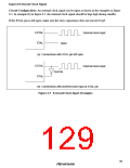
Figure 6.7
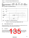
Note: * tDEXT includes a 10 tcyc RES pulse width (tRESW).
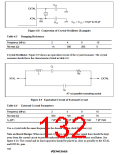
VCC
2.7 V
VIH
STBY
EXTAL
ø (internal or
external)
RES
tDEXT
*
Note: * tDEXT includes a 10 tcyc RES pulse width (tRESW).
Figure 6.7 External Clock Output Settling Delay Time
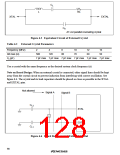
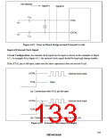
Oscillator Circuit (H8/3337SF)
6.2.2
If an external crystal is connected across the EXTAL and XTAL pins, the on-chip oscillator circuit
generates a system clock signal. Alternatively, an external clock signal can be applied to the
EXTAL pin.
Connecting an External Crystal
Circuit Configuration: An external crystal can be connected as in the example in figure 6.8.
Table 6.5 indicates the appropriate damping resistance Rd. An AT-cut parallel resonance crystal
should be used.
101

 RENESAS [ RENESAS TECHNOLOGY CORP ]