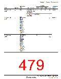
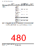
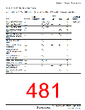
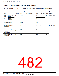
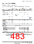
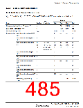
Section 22 Electrical Characteristics
22.3.4
A/D Converter Characteristics
Table 22.16 A/D Converter Characteristics
V
CC = 3.0 to 3.6 V, VSS = 0.0 V, Ta = -20 to +75°C/-40 to +85°C, unless otherwise indicated.
Values
Applicable Test
Symbol Pins
Condition
Reference
Unit Figure
Item
Min.
Typ. Max.
1
Analog power supply AVCC
voltage
AVCC
3.0
VCC
3.6
V
*
Analog input voltage AVIN
AN0 to
AN7
VSS – 0.3
—
AVCC + 0.3 V
Analog power supply AIOPE
current
AVCC
AVCC
AVCC
AVCC = 3.6 V —
fOSC
16 MHz
—
2.0
—
mA
=
2
AISTOP1
—
50
µA
*
Reference
value
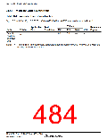
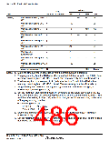
3
AISTOP2
—
—
—
—
5.0
µA
pF
*
Analog input
capacitance
CAIN
AN0 to
AN7
30.0
Permissible signal
source impedance
RAIN
AN0 to
AN7
—
—
10
—
5.0
10
—
kΩ
bit
tcyc
Resolution
(data length)
10
Conversion time
(single mode)
AVCC = 3.0 to 134
3.6 V
Nonlinearity error
Offset error
—
—
—
—
—
—
—
—
—
—
7.5
7.5
7.5
0.5
8.0
LSB
LSB
LSB
LSB
LSB
Full-scale error
Quantization error
Absolute accuracy
Notes: 1. Set AVCC = VCC when the A/D converter is not used.
2. AISTOP1 is the current in active and sleep modes while the A/D converter is idle.
3. AISTOP2 is the current at reset and in standby, subactive, and subsleep modes while the
A/D converter is idle.
Rev. 3.00 Sep. 10, 2007 Page 449 of 528
REJ09B0216-0300

 RENESAS [ RENESAS TECHNOLOGY CORP ]