Section 19 Band-Gap Circuit, Power-On Reset, and Low-Voltage Detection Circuits
Low Voltage Detection Interrupt (LVDI) Circuit
(When Internally Generated Voltage is used for Detection):
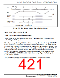
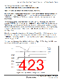
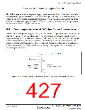
Figure 19.5 shows the timing of the operation of the LVDI circuit.
The LVDI circuit is enabled after a power-on reset, however, the interrupt request is disabled. To
enable the LVDI, the LVDDF bit and LVDUF bit in LVDSR must be cleared to 0 and then the
LVDDE bit or LVDUE bit in LVDCR must be set to 1. After that, the output settings of ports
must be made.
When the power-supply voltage falls below Vint (D) (Typ. = 3.7 V) voltage, the LVDI circuit
clears the LVDINT signal to 0 and sets the LVDDF bit to 1. If the LVDDE bit is 1 at this time, an
IRQ0 interrupt request is generated. In this case, the necessary data must be saved in the external
EEPROM and a transition to standby mode or subsleep mode must be made. Until this processing
is completed, the power supply voltage must be higher than the lower limit of the guaranteed
operating voltage.
When the power-supply voltage does not fall below the Vreset1 (Typ. = 2.3 V) voltage and rises
above the Vint (U) (Typ. = 4.0 V) voltage, the LVDI circuit sets the LVDINT signal to 1. If the
LVDUE bit is 1 at this time, the LVDUF bit in LVDSR is set to 1 and an IRQ0 interrupt request is
simultaneously generated.
If the power supply voltage (Vcc) falls below the Vreset1 (Typ. = 2.3 V) voltage, this LSI enters
low voltage detection reset operation (when LVDRE = 1).
Vint (U)
Vint (D)
Vcc
Vreset1
VSS
LVDINT
LVDDE
LVDDF
LVDUE
LVDUF
IRQ0 interrupt generated IRQ0 interrupt generated
Figure 19.5 Operational Timing of LVDI Circuit
Rev. 3.00 Sep. 10, 2007 Page 389 of 528
REJ09B0216-0300

 RENESAS [ RENESAS TECHNOLOGY CORP ]