Section 16 Serial Communication Interface 3 (SCI3)
16.4
Operation in Asynchronous Mode
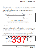
Figure 16.2 shows the general format for asynchronous serial communication. One character (or
frame) consists of a start bit (low level), followed by data (in LSB-first order), a parity bit (high or
low level), and finally stop bits (high level). Inside the SCI3, the transmitter and receiver are
independent units, enabling full-duplex. Both the transmitter and the receiver also have a double-
buffered structure, so data can be read or written during transmission or reception, enabling
continuous data transfer.
LSB
MSB
1
Serial
data
Parity
bit
Start
bit
Mark state
Transmit/receive data
7 or 8 bits
Stop bit
1 bit
1 bit
1 or
or none
2 bits
One unit of transfer data (character or frame)
Figure 16.2 Data Format in Asynchronous Communication
16.4.1
Clock
Either an internal clock generated by the on-chip baud rate generator or an external clock input at
the SCK3 pin can be selected as the SCI3’s serial clock, according to the setting of the COM bit in
SMR and the CKE0 and CKE1 bits in SCR3. When an external clock is input at the SCK3 pin, the
clock frequency should be 16 times the bit rate used.
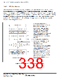
When the SCI3 is operated on an internal clock, the clock can be output from the SCK3 pin. The
frequency of the clock output in this case is equal to the bit rate, and the phase is such that the
rising edge of the clock is in the middle of the transmit data, as shown in figure 16.3.
Clock
1
1
0
D0 D1 D2 D3 D4 D5 D6 D7 0/1
1 character (frame)
Serial data
Figure 16.3 Relationship between Output Clock and Transfer Data Phase
(Asynchronous Mode) (Example with 8-Bit Data, Parity, Two Stop Bits)
Rev. 3.00 Sep. 10, 2007 Page 303 of 528
REJ09B0216-0300

 RENESAS [ RENESAS TECHNOLOGY CORP ]