Section 13 Timer Z
When the counter is incremented or decremented, the IMFA flag of channel 0 is set to 1, and when
the register is underflowed, the UDF flag of channel 0 is set to 1. After buffer operation has been
designated for BR, BR is transferred to GR when the counter is incremented by compare match
A0 or when TCNT_1 is underflowed. If the φ or φ/2 clock is selected by TPSC2 to TPSC0 bits,
the OVF flag is not set to 1 at the timing that the counter value changes from H'FFFF to H'0000. If
the φ/4 or φ/8 clock is selected by TPSC2 to TPSC0 bits, the OVF flag is set to 1.
3. Setting GR Value in Complementary PWM Mode: To set the general register (GR) or modify
GR during operation in complementary PWM mode, refer to the following notes.
A. Initial value
a. When other than TPSC2 = TPSC1 = TPSC0 = 0, the GRA_0 value must be equal to
H'FFFC or less. When TPSC2 = TPSC1 = TPSC0 = 0, the GRA_0 value can be set to
H'FFFF or less.
b. H'0000 to T – 1 (T: Initial value of TCNT0) must not be set for the initial value.
c. GRA_0 – (T – 1) or more must not be set for the initial value.
d. When using buffer operation, the same values must be set in the buffer registers and
corresponding general registers.
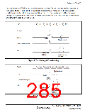
B. Modifying the setting value
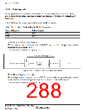
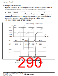
a. Writing to GR directly must be performed while the TCNT_1 and TCNT_0 values
should satisfy the following expression: H'0000 ≤ TCNT_1 < previous GR value, and
previous GR value < TCNT_0 ≤ GRA_0. Otherwise, a waveform is not output
correctly. For details on outputting a waveform with a duty cycle of 0% and 100%, see
C., Outputting a waveform with a duty cycle of 0% and 100%.
b. Do not write the following values to GR directly. When writing the values, a waveform
is not output correctly.
H'0000 ≤ GR ≤ T − 1 and GRA_0 − (T − 1) ≤ GR < GRA_0 when TPSC2 = TPSC1 =
TPSC0 = 0
H'0000 < GR ≤ T − 1 and GRA_0 − (T − 1) ≤ GR < GRA_0 + 1 when TPSC2 = TPSC1
= TPSC0 = 0
c. Do not change settings of GRA_0 during operation.
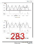
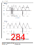
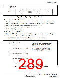
C. Outputting a waveform with a duty cycle of 0% and 100%
a. Buffer operation is not used and TPSC2 = TPSC1 = TPSC0 = 0
Write H'0000 or a value equal to or more than the GRA_0 value to GR directly at the
timing shown below.
•
•
To output a 0%-duty cycle waveform, write a value equal to or more than the GRA_0
value while H'0000 ≤ TCNT_1 < previous GR value
To output a 100%-duty cycle waveform, write H'0000 while previous GR value<
TCNT_0 ≤ GRA_0
Rev. 3.00 Sep. 10, 2007 Page 252 of 528
REJ09B0216-0300

 RENESAS [ RENESAS TECHNOLOGY CORP ]