Section 13 Timer Z
6. Examples of Buffer Operation
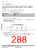
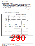
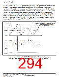
Figure 13.38 shows an operation example in which GRA has been designated as an output
compare register, and buffer operation has been designated for GRA and GRC.
This is an example of TCNT operating as a periodic counter cleared by compare match B.
Pins FTIOA and FTIOB are set for toggle output by compare match A and B.
As buffer operation has been set, when compare match A occurs, the FTIOA pin performs
toggle outputs and the value in buffer register is simultaneously transferred to the general
register. This operation is repeated each time that compare match A occurs.
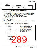
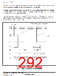
The timing to transfer data is shown in figure 13.39.
Counter is cleared by GBR compare match
TCNT value
GRB
H'0250
H'0200
H'0100
Time
H'0000
GRC
H'0200
H'0250
H'0100
H'0200
H'0200
H'0200
GRA
H'0100
FTIOB
FTIOA
Compare match A
Figure 13.38 Example of Buffer Operation (1)
(Buffer Operation for Output Compare Register)
Rev. 3.00 Sep. 10, 2007 Page 256 of 528
REJ09B0216-0300

 RENESAS [ RENESAS TECHNOLOGY CORP ]