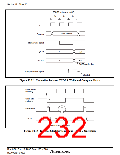
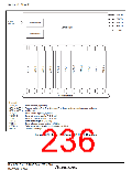
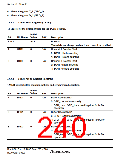
Section 13 Timer Z
FTIOA0
FTIOB0
FTIOC0
FTIOD0
φ, φ/2,
φ/4, φ/8
Clock select
Comparator
Control logic
ITMZ0
Module data bus
[Legend]
TCNT_0:
Timer counter_0 (16 bits)
GRA_0, GRB_0, General registers A_0, B_0, C_0, and D_0 (input capture/output compare registers:
GRC_0, GRD_0: 16 bits × 4)
TCR_0:
Timer control register_0 (8 bits)
TIORA_0:
TIORC_0:
TSR_0:
Timer I/O control register A_0 (8 bits)
Timer I/O control register C_0 (8 bits)
Timer status register_0 (8 bits)
TIER_0:
POCR_0:
ITMZ0:
Timer interrupt enable register_0 (8 bits)
PWM mode output level control register_0 (8 bits)
Channel 0 interrupt
Figure 13.2 Timer Z (Channel 0) Block Diagram
Rev. 3.00 Sep. 10, 2007 Page 202 of 528
REJ09B0216-0300

 RENESAS [ RENESAS TECHNOLOGY CORP ]