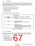
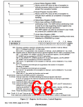
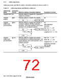
Saved Status Register (SSR)
31
31
0
0
Stores current SR value at time of exception to
indicate processor status in return to instruction
stream from exception handler.
SSR
SPC
Saved Program Counter (SPC)
Stores current PC value at time of exception to
indicate return address at completion of exception
handling.
Global Base Register (GBR)
0
Stores base address of GBR-indirect
31
GBR
addressing mode. The GBR-indirect addressing mode
is used for on-chip supporting module register area
data transfers and logic operations.
The GBR register can also be accessed in user mode.
Its contents are undefined after a reset.
31
0
Vector Base Register (VBR)
Stores base address of exception handling vector area.
Initialized to H'0000000 by a reset.
VBR
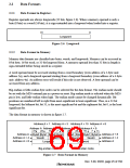
31 30 29 28 27
13 12 11 10 9 8 7
0 0
3
1 0
Status
register
(SR)
0 MD RB BL 0−−−−−−−−−−−−−−−−−−−−−−0 CL
M Q I3 I2 I1 I0 0 0 S T
MD: Processor operation mode bit: Indicates the processor operation mode as follows:
MD =1: Privileged mode; MD = 0: User mode
MD is set to 1 on generation of an exception or interrupt , and is initialized to 1 by a reset.
RB: Register bank bit: Determines the bank of general registers R0–R7 used in processing mode.
RB = 1: R0_BANK1−R7_BANK1 and R8−R15 are general registers, and R0_BANK0−
R7_BANK0 can be accessed by LDC/STC instructions.
RB = 0: R0_BANK0−R7_BANK0 and R8−R15 are general registers, and R0_BANK1−
R7_BANK1 can be accessed by LDC/STC instructions.
RB is set to 1 on generation of an exception or interrupt , and is initialized to 1 by a reset.
BL: Block bit
BL = 1: Exceptions and interrupts are suppressed. See section 4, Exception
Handling, for details.
BL = 0: Exceptions and interrupts are accepted.
BL is set to 1 on generation of an exception or interrupt , and is initialized to 1 by a reset.
CL: Cache lock bit
When set to 1, the cache lock function can be used.
M and Q bits: Used by the DIV0S/U and DIV1 instructions.
I3−I0 bits: Interrupt mask bits: 4-bit field indicating the interrupt request mask level.
I3−I0 do not change to the interrupt acceptance level when an interrupt is generated.
Initialized to B'1111 by a reset.
S bit: Used by the MAC instruction.
T bit: Used by the MOVT, CMP/cond, TAS, TST, BT, BF, SETT, CLRT, and DT instructions to
indicate true (1) or false (0).
Used by the ADDV/C, SUBV/C, DIV0U/S, DIV1, NEGC, SHAR/L, SHLR/L, ROTR/L, and
ROTCR/L instructions to indicate a carry, borrow, overflow, or underflow.
0 bits: These bits always read 0, and the write value should always be 0.
Note: The M, Q, S, and T bits can be set or cleared by special instructions in user mode.
Their values are undefined after a reset. All other bits can be read or written in privileged mode.
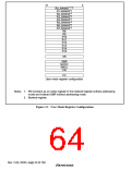
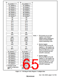
Figure 2.5 Register Set Overview, Control Registers
Rev. 5.00, 09/03, page 24 of 760

 RENESAS [ RENESAS TECHNOLOGY CORP ]