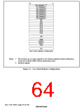
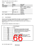
Register values after a reset are shown in table 2.1.
Table 2.1 Initial Register Values
*
Type
Registers
R0 to R15
SR
Initial Value
General registers
Control registers
Undefined
MD bit = 1, RB bit = 1, BL bit = 1,
I3–I0 = 1111 (H'F), reserved bits =
0, others undefined
GBR, SSR, SPC
VBR
Undefined
H'00000000
Undefined
H'A0000000
System registers
MACH, MACL, PR
PC
Note: * Register values are initialized at power-on reset or manual reset.
2.1.2
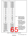
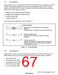
General Registers
There are 16 general registers, designated R0 to R15 (figure 2.3). General registers R0 to R7 are
banked registers, with a different R0–R7 register bank (R0_BANK0–R7_BANK0 or
R0_BANK1–R7_BANK1) being accessed according to the processor mode. For details, see
figures 2.1 and 2.2.
The general register configuration is shown in figure 2.3.
General Registers
31
0
R0*1 *2
R1*2
R2*2
R3*2
R4*2
R5*2
R6*2
R7*2
R8
Notes:
1. R0 functions as an index register in the indexed
register-indirect addressing mode and indexed
GBR-indirect addressing mode. In some instructions,
only R0 can be used as the source register or
destination register.
2.
R0–R7 are banked registers.
In privileged mode, SR.RB specifies which banked
registers are accessed as general registers
(R0_BANK0−R7_BANK0 or R0_BANK1−R7_BANK1).
R9
R10
R11
R12
R13
R14
R15
Figure 2.3 General Registers
Rev. 5.00, 09/03, page 22 of 760

 RENESAS [ RENESAS TECHNOLOGY CORP ]