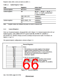
31
0
31
0
R0_BANK1*1 *2
R1_BANK1*2
R2_BANK1*2
R3_BANK1*2
R4_BANK1*2
R5_BANK1*2
R6_BANK1*2
R7_BANK1*2
R8
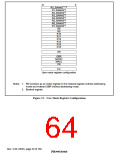
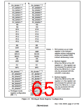
R0_BANK0*1 *3
R1_BANK0*3
R2_BANK0*3
R3_BANK0*3
R4_BANK0*3
R5_BANK0*3
R6_BANK0*3
R7_BANK0*3
R8
R9
R9
R10
R10
R11
R11
R12
R12
R13
R13
R14
R14
R15
R15
SR
SR
SSR
SSR
Notes:
1. R0 functions as an index
register in the indexed
GBR
MACH
MACL
PR
GBR
MACH
MACL
PR
register-indirect addressing
mode and indexed GBR-
indirect addressing mode.
2. Banked register
VBR
VBR
When the RB bit of the SR
register is 1, the register can
be accessed for general use.
When the RB bit is 0, it can
only be accessed with the
LDC/STC instruction.
PC
PC
SPC
SPC
R0_BANK0*1 *3
R1_BANK0*3
R2_BANK0*3
R3_BANK0*3
R4_BANK0*3
R5_BANK0*3
R6_BANK0*3
R7_BANK0*3
R0_BANK1*1 *2
R1_BANK1*2
R2_BANK1*2
R3_BANK1*2
R4_BANK1*2
R5_BANK1*2
R6_BANK1*2
R7_BANK1*2
3. Banked register
When the RB bit of the SR
register is 0, the register can
be accessed for general use.
When the RB bit is 1, it can
only be accessed with the
LDC/STC instruction.
a. Privileged mode
register configuration
(RB = 1)
b. Privileged mode
register configuration
(RB = 0)
Figure 2.2 Privileged Mode Register Configuration
Rev. 5.00, 09/03, page 21 of 760

 RENESAS [ RENESAS TECHNOLOGY CORP ]