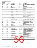
Number of Pins
FP-208C
FP-208E
BP-240A
Pin Name
I/O
Description
176
A11
CTS2/IRQ5/SCPT[7]
I
Transmit clear 2 / external interrupt
request / SCI input port
177
178
179
180
B11
D11
C11
B10
MCS[7]/PTC[7]/PINT[7] O / I/O / I Mask ROM chip select /
input/output port C / port interrupt
MCS[6]/PTC[6]/PINT[6] O / I/O / I Mask ROM chip select /
input/output port C / port interrupt
MCS[5]/PTC[5]/PINT[5] O / I/O / I Mask ROM chip select /
input/output port C / port interrupt
MCS[4]/PTC[4]/PINT[4] O / I/O / I Mask ROM chip select /
input/output port C / port interrupt
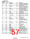
181
182
C10
D10
VssQ
—
Input/output power supply (0 V)
WAKEUP/PTD[3]
O / I/O
Standby mode interrupt request
notification / input/output port D
183
184
185
A10
C9
VccQ
—
Input/output power supply (3.3 V)
Reset output / input/output port D
RESETOUT/PTD[2]
MCS[3]/PTC[3]/PINT[3] O / I/O / I Mask ROM chip select /
O / I/O
D9
input/output port C / port interrupt
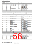
186
187
188
189
190
B9
A9
D8
C8
B8
MCS[2]/PTC[2]/PINT[2] O / I/O / I Mask ROM chip select /
input/output port C / port interrupt
MCS[1]/PTC[1]/PINT[1] O / I/O / I Mask ROM chip select /
input/output port C / port interrupt
MCS[0]/PTC[0]/PINT[0] O / I/O / I Mask ROM chip select /
input/output port C / port interrupt
DRAK0/PTD[1]
O / I/O
DMA request acknowledge /
input/output port D
DRAK1/PTD[0]
O / I/O
DMA request acknowledge /
input/output port D
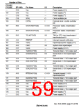
191
192
193
194
A8
D7
C7
B7
DREQ0/PTD[4]
DREQ1/PTD[6]
RESETP
I
I
I
I
DMA request / input port D
DMA request / input port D
Power-on reset request
CA
Chip activate (hardware standby
request signal)
195
196
197
A7
D6
C6
MD3
MD4
MD5
I
I
I
Area 0 bus width setting
Area 0 bus width setting
Endian setting
Rev. 5.00, 09/03, page 16 of 760

 RENESAS [ RENESAS TECHNOLOGY CORP ]