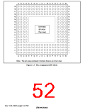
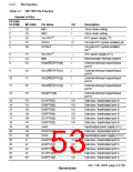
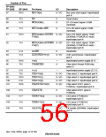
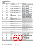
Number of Pins
FP-208C
FP-208E
BP-240A
Pin Name
I/O
Description
87
W12
BS/PTK[4]
O / I/O
Bus cycle start signal / input/output
port K
88
89
T13
U13
RD
O
O
Read strobe
WE0/DQMLL
D7–D0 select signal / DQM
(SDRAM)
90
91
V13
WE1/DQMLU/WE
O
D15–D8 select signal / DQM
(SDRAM)
W13
WE2/DQMUL/ICIORD/ O / I/O
D23–D16 select signal / DQM
(SDRAM) / PCMCIA I/O read /
input/output port K
PTK[6]
92
T14
WE3/DQMUU/ICIOWR/ O / I/O
D31–D24 select signal / DQM
(SDRAM) / PCMCIA I/O write /
input/output port K
PTK[7]
93
94
U14
V14
RD/WR
AUDSYNC/PTE[7]
O
Read/write
O / I/O
AUD synchronous / input/output
port E
95
96
W14
T15
VssQ
—
O
Input/output power supply (0 V)
CS0/MCS[0]
Chip select 0/mask ROM chip
select 0
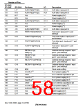
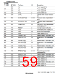
97
U15
T16
VccQ
—
Input/output power supply (3.3 V)
Chip select 2 / input/output port K
Chip select 3 / input/output port K
Chip select 4 / input/output port K
98
CS2/PTK[0]
CS3/PTK[1]
CS4/PTK[2]
CS5/CE1A/PTK[3]
O / I/O
O / I/O
O / I/O
O / I/O
99
W15
U16
W16
100
101
Chip select 5/CE1 (area 5
PCMCIA) / input/output port K
102
103
104
105
V15
V17
V16
T18
CS6/CE1B
O
Chip select 6/CE1 (area 6
PCMCIA)
CE2A/PTE[4]
CE2B/PTE[5]
CKE/PTK[5]
O / I/O
O / I/O
O / I/O
CE2 (area 5 PCMCIA) /
input/output port E
CE2 (area 6 PCMCIA) /
input/output port E
CK enable (SDRAM) / input/output
port K
Rev. 5.00, 09/03, page 12 of 760

 RENESAS [ RENESAS TECHNOLOGY CORP ]