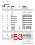
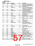
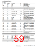
Number of Pins
FP-208C
FP-208E
BP-240A
Pin Name
I/O
Description
106
U18
RAS3L/PTJ[0]
O / I/O
Lower 32 M / 64 Mbytes address
(SDRAM) RAS / input/output port J
5
*
107
108
U19
R18
PTJ[1]
O / I/O
O / I/O
Input/output port J
CASL/PTJ[2]
Lower 32 M / 64 Mbytes address
(SDRAM) CAS / input/output port J
109
110
T19
T17
VssQ
—
Input/output power supply (0 V)
CASU/PTJ[3]
O / I/O
Lower 32 Mbytes address
(SDRAM) CAS / input/output port J
111
112
113
114
R19
U17
R17
R16
VccQ
—
Input/output power supply (3.3 V)
Input/output port J
PTJ[4]
I/O
PTJ[5]
I/O
Input/output port J
DACK0/PTD[5]
O / I/O
DMA acknowledge 0 / input/output
port D
115
P19
DACK1/PTD[7]
O / I/O
DMA acknowledge 1 / input/output
port D
116
117
118
P18
P17
P16
PTE[6]
I/O
Input/output port E
Input/output port E
PTE[3]
I/O
RAS3U/PTE[2]
O / I/O
Upper 32 Mbytes address
(SDRAM) RAS / input/output port
E
119
120
N19
N18
PTE[1]
I/O
Input/output port E
TDO/PTE[0]
O / I/O
Test data output / input/output
port E
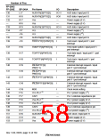
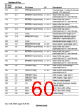
121
122
123
124
125
126
127
128
N17
N16
M19
M18
M17
M16
L19
L18
BACK
BREQ
WAIT
RESETM
ADTRG/PTH[5]
IOIS16/PTG[7]
ASEMD0/PTG[6]
ASEBRKAK/PTG[5]
O
Bus acknowledge
I
Bus request
I
Hardware wait request
Manual reset request
Analog trigger / input port H
IOIS16 (PCMCIA) / input port G
I
I
I
ASE mode 4 / input port G
*
I
O/I
ASE break acknowledge / input
port G
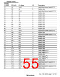
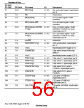
129
L16
PTG[4]/CK102
I
Input port G / clock output
Rev. 5.00, 09/03, page 13 of 760

 RENESAS [ RENESAS TECHNOLOGY CORP ]