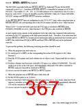
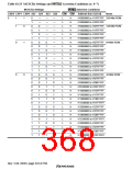
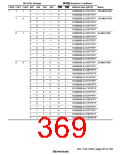
10.3.10 MCS[0] to MCS[7] Pin Control
The SH7709S is provided with pins MCS[0]–MCS[7] as dedicated CS pins for the ROM
connected to area 0 or 2. Assertion of MCS[0]–MCS[7] is controlled by settings in MCSCR0–
MCSCR7. This enables 32-, 64-, 128-, or 256-Mbit memory to be connected to area 0 or area 2.
However, only CS2/0 = 0 (area 0) should be used for MCSCR0. Table 10.15 shows MCSCR0–
MCSCR7 settings and MCS[0]–MCS[7] assertion conditions.
As the MCS[0]–MCS[7] pins are multiplexed as the PTC0–PTC7 pins, when using these pins as
MCS[0]–MCS[7], the corresponding bits in the PCCR register should be set to “other function.”
When CS2/0 = 0 in the MCSCR0 and when the PTC0 pin is switched to MCS[0] (when
PCOMD1–PCOMD0 are set to “other function”), the CS0 pin is also switched to MCS[0].
As port register writes operate on the peripheral clock, they take time compared with instruction
execution by the CPU operating on the high-speed internal clock. Therefore, if an instruction that
accesses MCS[1] to MCS[7] is located several instructions after an instruction that switches port C
to MCS, the switch from PTC[n] to MCSn and from CS0 to MCS[0] may not be performed
correctly.
To prevent this problem, the following switching procedure should be used.
•
When the program runs with cache on
(1) To switch port C to MCS, set the corresponding bits in the PCCR register to 00 ("other
function").
(2) Read the PCCR register and check whether the set value is read. Repeat until the set value is
read.
(3) Perform a dummy read from non-cacheable CS0 space (e.g. address H'A0000000). This will
result in an access to the CS0 space, and immediately afterward, CS0 will be switched to
MCS[0], and port C[n] will be switched to MCS[n].
(4) Access can now be made to the MCS[1] to MCS[7] spaces.
•
When the program runs in MCS[0] space with cache off
(1) Set the PCCR register as in (1) above.
(2) Place at least three NOP instructions after the instruction in (1). As a result, when the PCCR
register is rewritten, an access to the CS0 space will be generated, and immediately afterward,
CS0 will be switched to MCS[0], and port C[n] will be switched to MCS[n].
(3) Access can now be made to the MCS[1] to MCS[7] spaces.
Rev. 5.00, 09/03, page 323 of 760

 RENESAS [ RENESAS TECHNOLOGY CORP ]