Before mode register setting, a 100 µs idle time (depending on the memory manufacturer) must be
guaranteed after powering on requested by the synchronous DRAM. If the reset signal pulse width
is greater than this idle time, there is no problem in performing mode register setting immediately.
The number of dummy auto-refresh cycles specified by the manufacturer (usually 8) or more must
be executed. This is usually achieved automatically while various kinds of initialization are being
performed after auto-refresh setting, but a way of carrying this out more dependably is to set a
short refresh request generation interval just while these dummy cycles are being executed. With
simple read or write access, the address counter in the synchronous DRAM used for auto-
refreshing is not initialized, and so the cycle must always be an auto-refresh cycle.
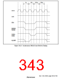
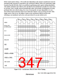
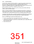
TRp1
TRp2
TRp3
TRp4
TMw1
TMw2
TMw3
TMw4
CKIO
A15 to A13
or A15 to A12
A11
A12 or A10
A9 to A2
CSn
RD/WR
RAS3U or RAS3L
CASU or CASL
D31 to D0
CKE
(High)
Figure 10.28 Synchronous DRAM Mode Write Timing
Rev. 5.00, 09/03, page 303 of 760

 RENESAS [ RENESAS TECHNOLOGY CORP ]