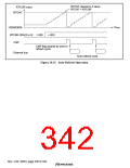
Power-On Sequence: In order to use synchronous DRAM, mode setting must first be performed
after powering on. To perform synchronous DRAM initialization correctly, the bus state controller
registers must first be set, followed by a write to the synchronous DRAM mode register. In
synchronous DRAM mode register setting, the address signal value at that time is latched by a
combination of the RAS, CAS, and RD/WR signals. If the value to be set is X, the bus state
controller provides for value X to be written to the synchronous DRAM mode register by
performing a write to address H'FFFFD000 + X for area 2 synchronous DRAM, and to address
H'FFFFE000 + X for area 3 synchronous DRAM. In this operation the data is ignored, but the
mode write is performed as a byte-size access. To set burst read/single write, CAS latency 1 to 3,
wrap type = sequential, and burst length 1 supported by the SH7709S, arbitrary data is written in a
byte-size access to the following addresses.
With 32-bit bus width:
Area 2
Area 3
CAS latency 1
CAS latency 2
CAS latency 3
FFFFD840
FFFFD880
FFFFD8C0
FFFFE840
FFFFE880
FFFFE8C0
With 16-bit bus width:
Area 2
Area 3
CAS latency 1
CAS latency 2
CAS latency 3
FFFFD420
FFFFD440
FFFFD460
FFFFE420
FFFFE440
FFFFE460
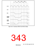
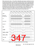
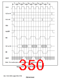
Mode register setting timing is shown in figure 10.28.
As a result of the write to address H'FFFFD000 + X or H'FFFFE000 + X, a precharge all banks
(PALL) command is first issued in the TRp1 cycle, then a mode register write command is issued
in the TMw1 cycle.
Address signals, when the mode-register write command is issued, are as follows:
32-bit bus width:
A15–A9 = 0000100 (burst read and single write)
A8–A6 = CAS latency
A5 = 0 (burst type = sequential)
A4–A2 = 000 (burst length 1)
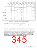
16-bit bus width:
A14–A8 = 0000100 (burst read and single write)
A7–A5 = CAS latency
A4 = 0 (burst type = sequential)
A3–A1 = 000 (burst length 1)
Rev. 5.00, 09/03, page 302 of 760

 RENESAS [ RENESAS TECHNOLOGY CORP ]