9.9
Notes on Board Design
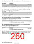
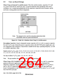
When Using an External Crystal Resonator: Place the crystal resonator, capacitors CL1 and
CL2 close to the EXTAL and XTAL pins. To prevent induction from interfering with correct
oscillation, use a common grounding point for the capacitors connected to the resonator, and do
not locate a wiring pattern near these components.
Avoid crossing
signal lines
CL1
CL2
EXTAL
XTAL
SH7709S
Note: The values for CL1 and CL2 should be determined after
consultation with the crystal manufacturer.
Figure 9.4 Points for Attention when Using Crystal Resonator
Decoupling Capacitors: Insert a laminated ceramic capacitor of 0.1 to 1 µF as a passive capacitor
for each VSS/VCC pair. Mount the passive capacitors close to the SH7709S power supply pins, and
use components with a frequency characteristic suitable for the chip’s operating frequency, as well
as a suitable capacitance value.
Digital system VSS/VCC pairs: 19-21, 27-29, 33-35, 45-47, 57-59, 69-71, 79-81, 83-85, 95-97, 109-
111, 132-134, 153-154, 161-163, 173-175, 181-183, 205-208
On-chip oscillator VSS/VCC pairs: 3-6, 145-147, 148-150
Note: The pin numbers above apply to LQFP and HQFP packages.
When Using a PLL Oscillator Circuit: Keep the wiring from the PLL VCC and VSS connection
pattern to the power supply pins short, and make the pattern width large, to minimize the
inductance component. Ground the oscillation stabilization capacitors C1 and C2 to VSS (PLL1)
and VSS (PLL2), respectively. Place C1 and C2 close to the CAP1 and CAP2 pins and do not
locate a wiring pattern in the vicinity. In clock mode 7, connect the EXTAL pin to VCC or VSS and
leave the XTAL pin open.
Rev. 5.00, 09/03, page 220 of 760

 RENESAS [ RENESAS TECHNOLOGY CORP ]