8.4
Standby Mode
8.4.1
Transition to Standby Mode
To enter standby mode, set the STBY bit to 1 in STBCR, then execute the SLEEP instruction. The
chip switches from the program execution state to standby mode. In standby mode, power
consumption is greatly reduced by halting not only the CPU, but the clock and on-chip peripheral
modules as well. The clock output from the CKIO and CKIO2 pins also halts. CPU and cache
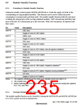
register contents are held, but some on-chip peripheral modules are initialized. Table 8.4 lists the
states of registers in standby mode.
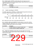
Table 8.4 Register States in Standby Mode
Module
Registers Initialized
Registers Retaining Data
All registers
Interrupt controller (INTC)
—
—
On-chip clock pulse generator
(OSC)
All registers
User break controller (UBC)
Bus state controller (BSC)
Timer unit (TMU)
—
All registers
All registers
Registers other than TSTR
All registers
—
—
TSTR register
Realtime clock (RTC)
A/D converter (ADC)
D/A converter (DAC)
—
All registers
—
All registers
The procedure for moving to standby mode is as follows:
1. Clear the TME bit in the WDT’s timer control register (WTCSR) to 0 to stop the WDT. Clear
the WDT’s timer counter (WTCNT) to 0 and the CKS2–CKS0 bits in the WTCSR register to
appropriate values to secure the specified oscillation settling time.
2. After the STBY bit in the STBCR register is set to 1, a SLEEP instruction is executed.
3. Standby mode is entered and the clocks within the chip are halted. The STATUS1 pin output
goes low and the STATUS0 pin output goes high.
Rev. 5.00, 09/03, page 188 of 760

 RENESAS [ RENESAS TECHNOLOGY CORP ]